1
\$\begingroup\$

I'm designing a PCB which uses the ESP32-D0WDQ6 WiFi chip (not the entire module!). I want to add the uFL connector so that I can connect an antenna instead of using the PCB trace antenna.

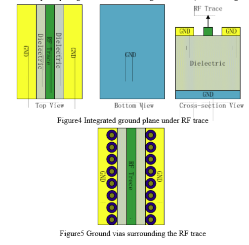
Now, I searched for this before and found this in a datasheet of SIM9000 which is related to designing a 3G module which an antenna connector:

2 layer example

This shows the recommended layout for the 3G module's antenna feed line on a 2 layer board.

My question is, can I use the same idea with my ESP32 chip on a 4 layer board? (I have inner layers dedicated to ground and power plane each)

More specifically, is it needed that the inner copper pours (ground and power planes on inner layers) be left under the antenna feed line and the uFL connector itself or do I have to remove them?

\$\endgroup\$
1
  • \$\begingroup\$ Keep the ground under the RF trace. You can use the same guidelines as for the 2 layer board. But you need to recalculate the the trace width and ground clearance for your 4 layer stackup. You can use the power place as the reference for the RF return current, but I would avoid it. \$\endgroup\$
    – Mike
    Commented Dec 9, 2017 at 19:25

2 Answers 2

1
\$\begingroup\$

The coplanar waveguide on ground plane you have found can be used in your application. BUT :

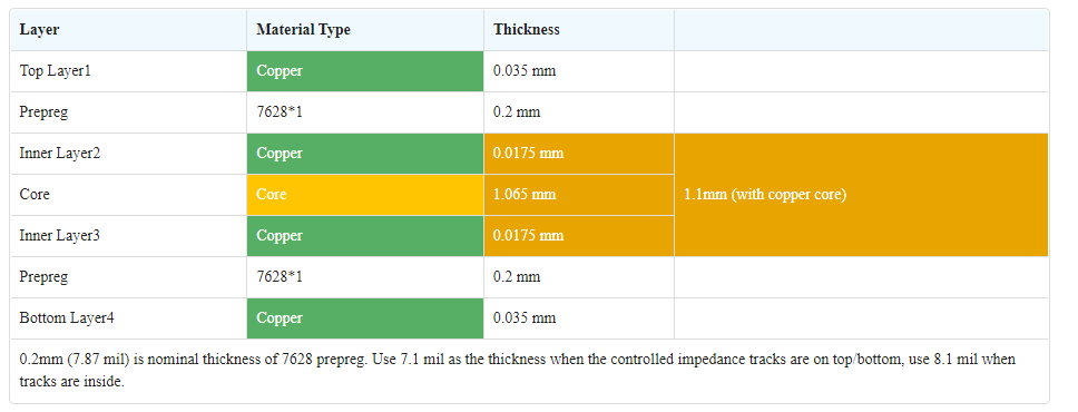
Be aware, that your stack up will certainly be build upon two PCB built with a core, then pressed again a pre-preg fabric to bind them. Or the other way around. But this pre-preg may or may not have the same dielectric properties of the two previous core or vice-versa. This dielectric jump, must be accounted for during development. And shall be if possible minimized. This page from JLCPCB illustrate well this problem : link enter image description here

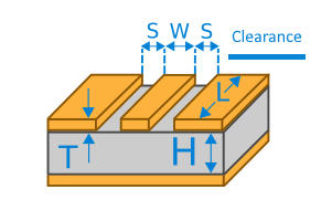
Moreover, when designing the coplanar waveguide on ground plane you had nothing between the excited center line, and the GND plane. This must be kept, so you are right when you say that every inner copper plane, in your transmission line must be empty. The thumb rule for this clearance dimension is to keep the copper layer at a distance of minimum 3 times the isolation between your GND and the excitation trace. Meaning, that starting at yours vias and going outward, you want a clearance zone 3*Isolation before starting pouring your copper power plan or any traces.

Hope the folowing schematic is clearer that the explanation :

enter image description here

\$\endgroup\$
-1
\$\begingroup\$

You can use the same coplanar waveguide. You'll want to get Saturn PCB Toolkit to calculate the appropriate geometry for the shorter distance to the inner ground plane. You would be best served to keep this trace on the same outer layer, and keep a solid ground plane under it.

\$\endgroup\$
3
  • \$\begingroup\$ As far as I remember Saturn PCB TOolkit doesn't do Grounded Coplanar Wave Guides, which is the transmission line topology shown. Perhaps it's better to use some online calculator for that. \$\endgroup\$
    – Mike
    Commented Dec 9, 2017 at 19:38
  • \$\begingroup\$ @Mike Not sure how far back that was, but it's been a feature for at least the last several versions. \$\endgroup\$
    – Matt Young
    Commented Dec 9, 2017 at 19:46
  • \$\begingroup\$ Thank you for your answer, I will calculate and adjust the trace width to match the 50ohm impedance today. I just have two more questions. 1. Would this design be alright? i.imgur.com/HTFzmUT.png 2. On the image on the top left, you can see the soldering pad for a triac (part of a crowbar circuit), that is its GND pad, is it alright if I extend the top ground pour of the feed line "shield" onto it as well or should I connect it to ground separately using vias? \$\endgroup\$
    – caffeine93
    Commented Dec 10, 2017 at 12:31

Your Answer

By clicking “Post Your Answer”, you agree to our terms of service and acknowledge you have read our privacy policy.

Not the answer you're looking for? Browse other questions tagged or ask your own question.