4
\$\begingroup\$

In the answers to my previous question "RF Design Basics", there are explanations about the purpose of a golden ring around the PCB edge and around some parts (functional blocks) within the PCB.

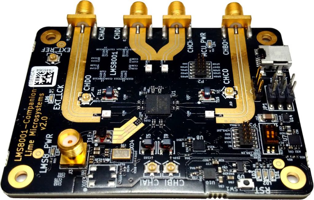
However, I want to know: What is the purpose of the golden area surrounding the RF traces, like in the Lime Microsystems board below? I suppose it is, again, used as a shield, but does it have to be golden in this case when it is not intended for shell mounting? Will the masked (painted) copper with the proper via stitching around do the same thing? And, is there some rule that defines the width of the surrounding area that have to be golden?

Lime Microsystems PCB

\$\endgroup\$

2 Answers 2

5
\$\begingroup\$

This is either co-planar waveguide, or co-planar waveguide above ground. There appear to be filled vias in the top ground, so these almost certainly go a ground in the next layer down. CPWaG is a nice construction that allows easy transition to microstrip, to connectors, and to surface mount components.

This is a demo board for a component. Such a board may simply be measured by the customer. Or, it might be modified, or even built into a prototype demo system. As such, it has to be easy to modify and probe.

There are several reasons why the area adjacent to the line might be left free of solder resist, which was uppermost in the mind of the designer is a matter for speculation. In no particular order ...

a) For the look of the thing. You can easily see the 'keep out' area, that you need to keep free of stray wires, rats nest components, blobs of glue or labels. It also looks nice, for much the same reason that you'd leave a carbon-fibre component with its cool black weave on your motorbike visible.

b) RF performance. Solder resist in this area would change the RF performance very slightly. Whether it's enough to be significant depends on the operating frequency. Those connectors have ground tabs in a position that suggests it's nowhere near their RF limit, so I think the effect would be pretty minimal.

c) To allow easy mounting of components for attenuators etc. The beauty of CPW, whether above ground or not, is that shunt components like resistors for attenuators, diodes for switches, inductors for dc return to ground, or 6pin SOT363 components can be mounted between the line and grounds. The same goes for the ground of any coaxial probe. Much easier if you don't have to scrape solder resist off first before adding your own circuitry to the board.

\$\endgroup\$
5
  • \$\begingroup\$ Does the plating / finish matter for RF performance? I suspect not significantly. \$\endgroup\$
    – vicatcu
    Commented Dec 28, 2017 at 15:17
  • \$\begingroup\$ Solder mask can effect the impedance of RF transmission lines (Stripline, Microstrip, Coplanar Waveguide, etc) This can be managed with appropriate modelling in CAD tools, or you could just leave solder mask off. As with everything in Engineering, whether the effect of solder mask on a circuit will depend on the specifications you're trying to meet. \$\endgroup\$
    – rfdave
    Commented Dec 28, 2017 at 16:47
  • 3
    \$\begingroup\$ @Neil_UK - I agree, solder mask can effect the impedance. Here is an app note from Rogers comparing a microstrip transmission line with/without a solder mask, with ~ 15 to 20% more insertion loss with a solder mask. rogerscorp.com/documents/2341/acm/articles/… \$\endgroup\$
    – rfdave
    Commented Dec 28, 2017 at 21:20
  • \$\begingroup\$ In part b), what about the position of the connectors' ground tabs suggests they are not operating near their maximum RF frequency? \$\endgroup\$
    – airdas
    Commented Feb 21, 2019 at 11:08
  • 1
    \$\begingroup\$ @airdas They are a long way from the inside surface of the outer of the coax. It's at this surface that the return current is flowing. The fact that the current has to flow across the surface of the flange to these tabs before it gets to the board ground introduces a huge series inductance. A high frequency connector puts the tabs right at the coax outer, to minimise this distance. \$\endgroup\$
    – Neil_UK
    Commented Feb 21, 2019 at 17:09
3
\$\begingroup\$

This answer just covers the part of the question about the reason for gold plating.

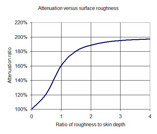
The gold finish provides a smoother surface than most other available finishes. Roughness increases the loss of microwave transmission lines. See this article on surface roughness for more details. The gold on the top of the lines helps some, but for coplanar waveguide in your picture, the roughness of the thin sides of the copper trace are probably important.

The roughness loss is graphed against the ratio of the roughness to the skin depth. The skin depth is inversely proportional to the square root of frequency, so higher frequencies call for smoother materials. This graph is from the microwaves101.com article linked above.

Ratio of roughness to skin depth

In some PCB materials, a microscopic view of the cross-section of the the copper conductor layer forms what look like nails penetrating the plastic. These nails help the copper stick to the board, but they increase microwave loss. Microwave designers choose materials based on the dielectric losses at high frequency and also the material smoothness and uniformity. This can make microwave circuits more costly and fragile, and extra care has to be taken to keep them from falling apart. Imagine trying to get copper to stick to Teflon! It is an example of a low loss microwave material with an adhesion challenge.

\$\endgroup\$

Your Answer

By clicking “Post Your Answer”, you agree to our terms of service and acknowledge you have read our privacy policy.

Not the answer you're looking for? Browse other questions tagged or ask your own question.