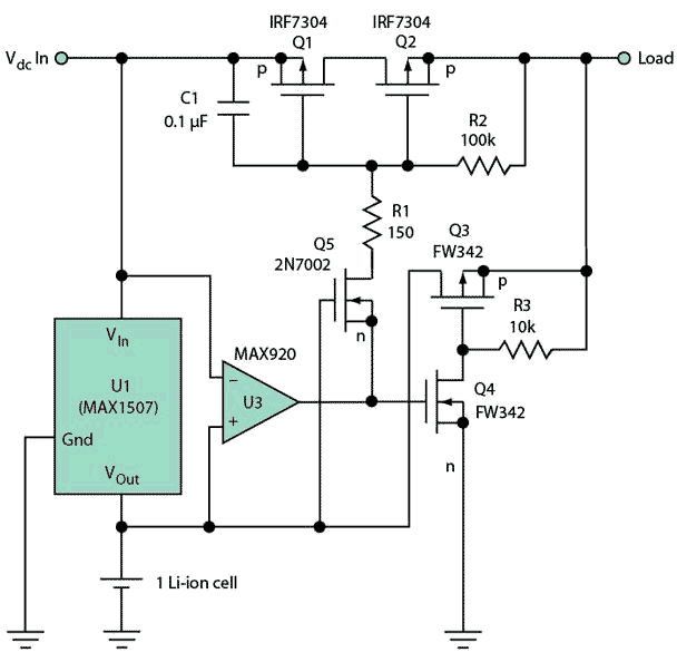
The question is how does this circuit works, special how does Q5
works? and C1, R2.
Q5 is operated as a "common gate" amplifier. When the comparator output goes low (ground/0 volts) the lithium cell that was biasing the gate now has its full voltage across gate and source of Q5 and this switches it on.
This drags the gates of Q1 (input voltage polarity protection) and Q2 (the main switch) down to 0 volts and turns both those devices on. R2 biases off Q2 so it will properly turn off when Q5 is inactive.
C1 is, I suspect a little bit of noise protection or just a means of slowing down the combination of Q1 and Q2 when they turn off i.e. C1 will hold the previously low voltage on their gates low whilst being slowly discharged by R2.
Is there a mistake in use of Q1 (part of IRF7304)? I suppose its D-S
inversion.
No, I believe it's there for reverse input polarity protection.
How to roughly estimate the switching voltage and time for this
circuit when Vdc lost)?
It's pretty much determined by C1 being discharged by R2 but I would urge you to consider simulating this in your favourite free simulator.
Read the full MAXIM description for this circuit operation here

