14
\$\begingroup\$

Wave soldering

I am trying to understand how wave soldering works. Unfortunately the Wikipedia article has has left me unsure about the process:

  1. Is the entire board with its components quasi-immersed in liquid solder while it passes through the wave? (If not, the following question probably make no sense.)
  2. If the board cuts into the wave, how is the wave maintained?
  3. Why does this not leave superflous solder residue on the board?

Double-Sided SMT soldering

How are double sided boards with SMT components soldered? How is it prevented that the components on one side fall off?

\$\endgroup\$

4 Answers 4

18
\$\begingroup\$

The wave only contacts the bottom side of the PCB.

Once upon a time, a wave solder machine was used to solder SMT parts on the bottom side of the PCB but this is not used as much anymore in favor of more modern techniques.

Here is the rough process for soldering PCB's with SMT parts on both sides, and through hole (TH) parts on the top side only.

A. The bare PCB is turned "bottom side up". A solder paste is pressed through a stencil and onto the pads of the PCB. A pick and place machine places the parts onto the bottom side. The PCB is ran through an oven (hot-air convection or an IR oven) to melt the solder and attach the parts.

An optional step is to place a small drop of glue under the parts. Solder paste first, then glue, then the parts are put onto the PCB and soldered. This glue helps keep the parts from falling off during a later step.

B. The board is turned over (top side up), and the same process is repeated for all SMT parts on the top side of the PCB. By that I mean solder paste, parts placed, then through the oven. No glue is needed.

During step B, the parts on the bottom of the PCB don't fall off. Obviously if they are glued down then they are stuck there, but most companies do not use glue. Without glue, the surface tension from the molten solder is enough to hold the parts in place. Some parts, particularly heavy parts without many pins, might not work with this technique since there is not enough surface tension to hold the parts on.

C. All of the through-hole parts are then placed on the top side of the PCB. A solder pallet is attached to the bottom of the PCB. The PCB is ran through a wave solder machine to solder all the TH parts.

Note: A solder pallet is basically a shield to protect the SMT parts from being removed in the wave. They are custom made for each PCB, and have holes and contours to expose the TH parts while shielding the SMT parts. The PCB must be designed with the solder pallet in mind, since you can't place the bottom side SMT parts too close to the TH parts and the SMT parts cannot be too tall.

A relatively new technique for TH parts is to skip the wave solder machine completely. Back in step B, solder paste is placed on the TH pads (and in the holes) and the TH parts are inserted and soldered in the oven with the rest of the SMT parts. Some companies, like Motorola, have gotten rid of their wave solder machines in favor of this method. But most companies still use the older technique of using a wave solder machine with solder pallet.

There are, of course, many variations of this entire process. I have just given a simple and brief overview. But it is fairly consistent with the way current manufacturing processes work today (things were different even just 10 years ago).

\$\endgroup\$
10
\$\begingroup\$

wave soldering
For wave soldering the PCB passes over a bath of molten solder where the solder is pushed up so that it strikes along the bottom side of the PCB. You'll need a solder resist mask to prevent to have solder over all the copper.

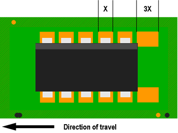
Note that also SMDs can be wave soldered, but then the orientation of the parts is important. Some parts have to be placed perpendicular to the wave direction. Fine pitch parts like 0.4 mm QFPs can't be wave soldered because all the pins will be shorted, but QFPs with a higher pitch can. They need "solder thieves", which are solder pads at the end of a row of pins to gather residual solder.

enter image description here

A QFP may have to be placed at a 45° angle, and will have the solder thieves at one of the corners:

enter image description here

The wave direction is important during PCB layout and panelization, and the production engineer should get clear instructions on it.

reflow soldering
SMDs for two-sided placement are glued on one side. After solder paste is applied with a stencil a glue dot machine places glue dots for the parts (at an incredible rate of more than 10 per second). Then the parts are placed, the panel is flipped over, and the other side gets solder paste and component placement.

\$\endgroup\$
1
  • 2
    \$\begingroup\$ When wave soldering SMD components, how to avoid the solder to "touch" the actual component and solder only the pins? Are solder pallets are used for this? \$\endgroup\$ Commented Dec 7, 2018 at 8:10
8
\$\begingroup\$

I do not know what you have pictured in your mind about solder wave, but it is a relatively simple process.

The circuit board is set between 2 conveyor chains. The chains are simple roller chains but have "fingers" about 2 inches long. One conveyor is movable to accept different size circuit boards. They are also inclined maybe 7 degrees. The circuit boards are set on one end of the conveyor, they pass over a fluxer that applies solder flux to the connections to be soldered. The solder is contained in a tank that is HOT and the solder is in a liquid state. There are pumps that actually pump the solder within its own tank and creates the wave. Surface tension is very visible and the bottom of the circuit being soldered comes in contact with the solder as it passes over the wave. This is for through-hole soldering only and is not used for SMT components. Any flux residue is washed off in a commercial board washer.

SMT components are a different story. The bare circuit board is run through a type of screen printer and solder paste is applied through a stencil. The components are placed with a Pick & Place machine, then the boards are run through a reflow oven. If the board is double-sided, a small amount of epoxy is placed under each component so it will not fall off the board during the reflow (oven) process of the second side. Hope I was able to answer your questions.

\$\endgroup\$
0
\$\begingroup\$

This is a somewhat archaic method where the entire bottom of the board is drawn along a flowing pool of solder: https://www.youtube.com/watch?v=inHzaJIE7-4

Newer methods include a small cnc solder fountain that is applied to the individual solder points on the board, rather than a bath that the entire unit runs through.

The pros and cons of each, I'm not entirely sure.

Also, here's a video of a pick and place machine: https://www.youtube.com/watch?v=tn0EKtLOVx4

\$\endgroup\$

Your Answer

By clicking “Post Your Answer”, you agree to our terms of service and acknowledge you have read our privacy policy.

Not the answer you're looking for? Browse other questions tagged or ask your own question.