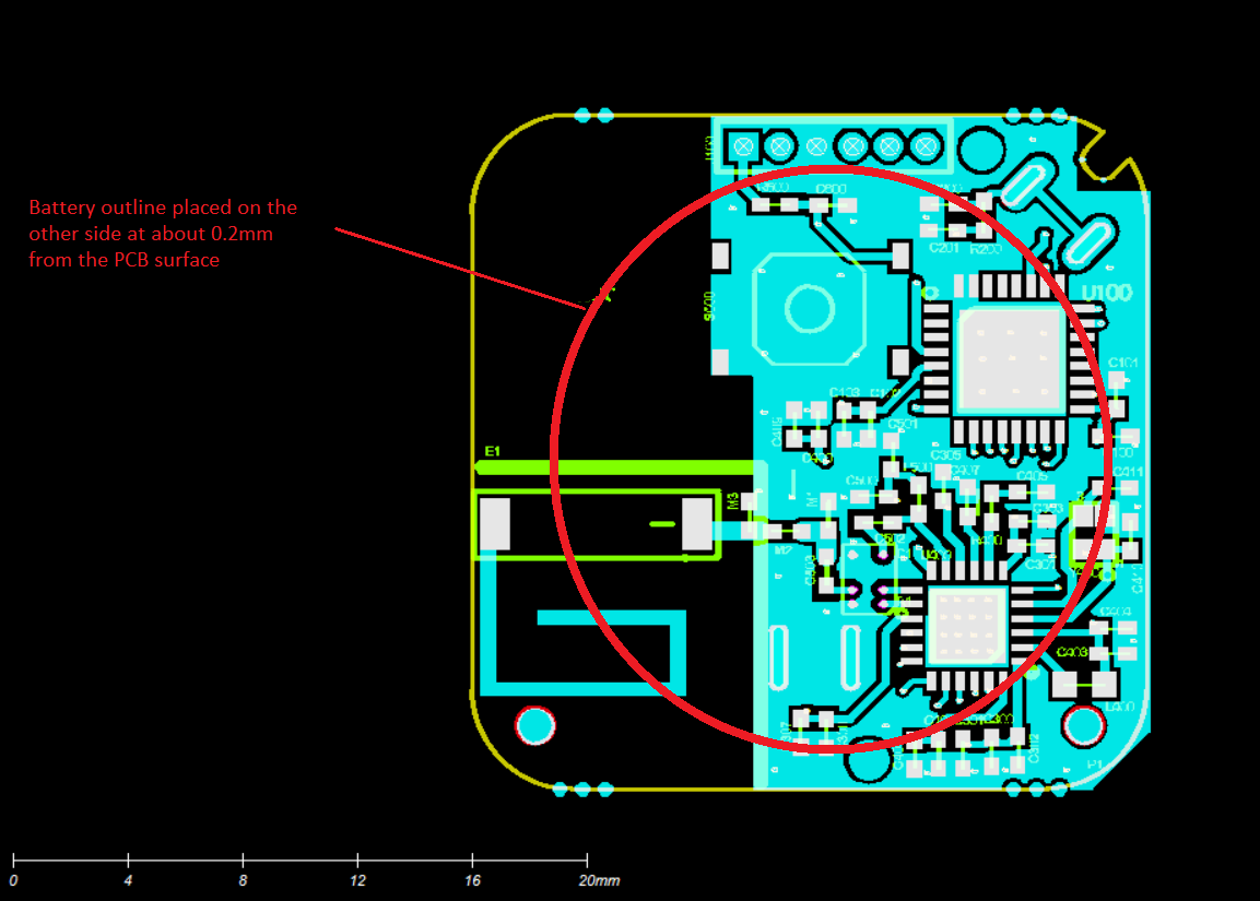
My new PCB design is about 25 mm * 25 mm, this is not enough for a proper 868 MHz antenna ground plane, I am using the 0868AT43A0020 chip antenna where at least a 20 mm * 40 mm GND plane is required. The first prototypes confirm the weak RF performances. what is the standard practice when it comes to dipole antenna when the ground plane of the PCB is extremely small and not sufficient?
\$\begingroup\$
\$\endgroup\$
19
-
2\$\begingroup\$ why are you asking about dipoles when you deal with a chip antenna? A proper dipole will be much, much larger. \$\endgroup\$– Marcus MüllerCommented Jun 27, 2018 at 10:10
-
1\$\begingroup\$ The standard practice is to live with the shortfall or make the GP more suitable. BTW a half wave dipole antenna does not need a GP. A quarter wave monopole antenna does. \$\endgroup\$– Andy akaCommented Jun 27, 2018 at 10:39
-
2\$\begingroup\$ are you sure that that ground plane is needed? \$\endgroup\$– Jasen Слава УкраїніCommented Jun 27, 2018 at 10:40
-
1\$\begingroup\$ @TarikMokafih How are you measuring Total Radiated Power? Could you try and move the battery to the right - away from the antenna. Its now directly under the antenna and it is affecting it for sure. \$\endgroup\$– user94729Commented Jul 2, 2018 at 11:14
-
1\$\begingroup\$ @TarikMokafih Are you measuring a 3D sphere to get the TRP. Or are you measuring ERP, or EIRP. Are you sure that you are actually measuring in the direction of max antenna gain? \$\endgroup\$– user94729Commented Jul 3, 2018 at 6:22
|
Show 14 more comments
1 Answer
\$\begingroup\$
\$\endgroup\$
3
the only place in the document you link to that contains 20×40mm² dimensions is the eval board. That's just "randomly" in that size.
What's important is that the chip is offset some 1mm from the edge of a ground plane, and that you have the folded whip as specified, and that you properly match your antenna, as specified in multiple places of the data sheet. My guess is you forgot the latter.
-
\$\begingroup\$ are these the matching instructions? johansontechnology.com/tuning.html \$\endgroup\$ Commented Jun 27, 2018 at 10:46
-
\$\begingroup\$ all design instructions are followed and the antenna was matched. However I still get poor RF performance compared to bigger PCBs \$\endgroup\$ Commented Jun 27, 2018 at 11:32
-
1\$\begingroup\$ @Tarik, you'll probably need to share your schematic and layout to get a useful answer then. Also are you enclosing the pcb in a housing of some kind? \$\endgroup\$ Commented Jun 27, 2018 at 13:52

