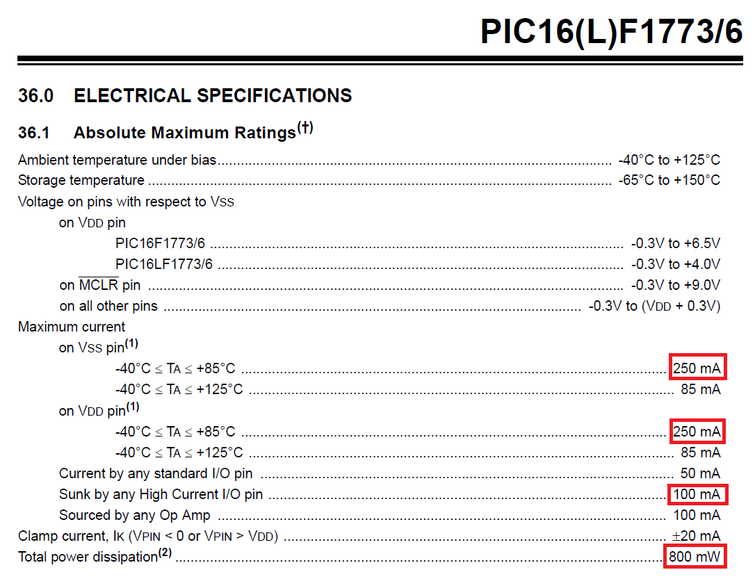
MCUs have maximum source/sink capabilities per GPIO, maximum source/sink currents through the VDD/VSS pins, and have maximum total power dissipation in function of package.
These parameters are all explicitly declared in the datasheet. For instance, the high current ports on the PIC16 family can output 100mA per pin, the sum of all currents going through the VDD/VSS pins must be less than 250mA, and the package can dissipate 800mW.

Does this mean that at any given time the GPIOs can never output more than 100mA on the high current pins, or that this limit can be surpassed (i.e. having a short high current pulse) as long as the total package power dissipation is less than 800mW?
EXAMPLE
Let me give an example to better illustrate my question.
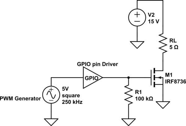
Suppose I have this circuit:

simulate this circuit – Schematic created using CircuitLab
The datasheet for the IRF8736 states that the input capacitance (Ciss) is 2315pF @ Vds=15V (i.e. non-zero) and a gate resistance of 2.2Ohms, so the instant the GPIO signal goes high, the instantaneous current will be:
\$i = V / R\$
\$i = (Vdriver - Vgate) / Rgate\$
\$i = (5V - 0V) / 2.2Ohms\$
\$i = 2.27A\$
This is way larger than the 100mA maximum allowable current for the GPIO pin.
However, if we look at the power consumed by the driver to drive this signal:
\$Pdriver = Vgate * Qg * Fsw\$
\$Pdriver = 5V * 26nC * 250kHz\$
\$Pdriver = 32.5mW\$
Which is far below the total 800mW allowable by the MCU.
So in this particular case, which parameter should be followed to respect the limits of the MCU? The maximum allowable GPIO pin current, or the total allowable package dissipated power? I wish there was a total allowable power dissipation per GPIO.
