0
\$\begingroup\$

I was watching a tutorial about this MCU (TM4C123 dev board), but I don't understand where they got the memory location address from. All they are doing is switching the built in red LED on the board on and off.

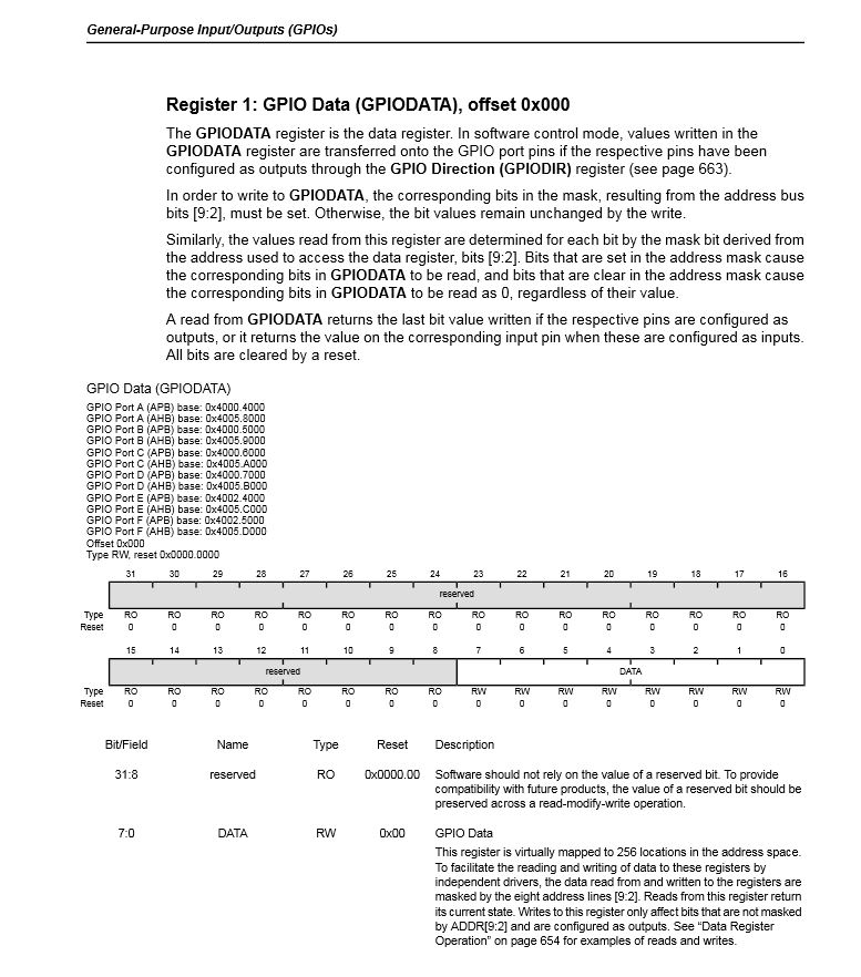
They are setting bit 1 in the GPIODATA register (see attached image of the datasheet for this register) with the address 0x400253FCU and writing a hex value of 0x20U to it. They then clear the bit by writing 0x0U to the same address to switch the LED off (there are time delays in between off course).

My question is, that I don't understand where the offset of '3FC' comes from? I am used to just writing down the offset given in the datasheet. In this case I thought it would have been 0x40025000U.

I think I am misunderstanding something due to the fact that this is a 32-bit MCU.

Thanks for all help everyone.

enter image description here

\$\endgroup\$

1 Answer 1

3
\$\begingroup\$

If you read the section you quoted. You’ll see that bits [9:2] of the address are used as a mask to allow changing only some of the bits on a write. Those bits correspond to a hex value of 3FC. Therefore, they are enabling writes to all 8 bits.

If they wanted to make sure that only the bit corresponding to the LED were changed, the 3FC would be changed to the bit position, shifted left 2 bits.

This is actually a very nice feature as it allows separate execution threads to interact with different bits without having to go use read-modify-write which could clobber the same in another thread.

\$\endgroup\$
9
  • \$\begingroup\$ Sorry, I still don't understand. What does it mean that bits [9:2] are used as a mask? \$\endgroup\$
    – David777
    Commented Sep 4, 2019 at 21:19
  • 1
    \$\begingroup\$ In this context, a mask is controlling which bits can be modified by a write operation. If you use a mask of 0x20, only that one bit will be set, regardless of if the written value id 0x20, 0x22 or 0xFF. All of the other bits will remain unchanged. A mask of 0xFF will allow all 8 bits to be modified. Anyway, the mask is encoded into the register address. Bits [10:31] actually specify the register. Bits [2:9] encode the mask. So t compute the address to use, it's base[=0x40025000] + (mask << 2). If mask is 0xFF (allow all bits), this computes ox 0x400253FC. [continued] \$\endgroup\$
    – DoxyLover
    Commented Sep 4, 2019 at 22:28
  • 2
    \$\begingroup\$ If you wanted to only allow the one LED bit to be modified, you would make the mask 0x20. With the left shift, you'd end up with 0x40025080. If you just used 0x40025000, writes would be ignored since the mask is 0x00. \$\endgroup\$
    – DoxyLover
    Commented Sep 4, 2019 at 22:31
  • 1
    \$\begingroup\$ Ah, sorry. That’s a notation used commonly in electronic design. Yes, counting 0 as lest significant bit, [2:9] means bits 2 through 9, corresponding to 0x3FC if the bits are all ones. \$\endgroup\$
    – DoxyLover
    Commented Sep 5, 2019 at 12:37
  • 1
    \$\begingroup\$ Actually, it’s a data mask, just encoded in the address bits, but yes. \$\endgroup\$
    – DoxyLover
    Commented Sep 5, 2019 at 19:21

Your Answer

By clicking “Post Your Answer”, you agree to our terms of service and acknowledge you have read our privacy policy.

Not the answer you're looking for? Browse other questions tagged or ask your own question.