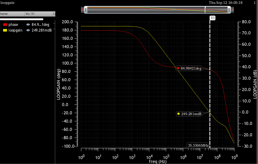
The Bode plot of the loop is as shown here:
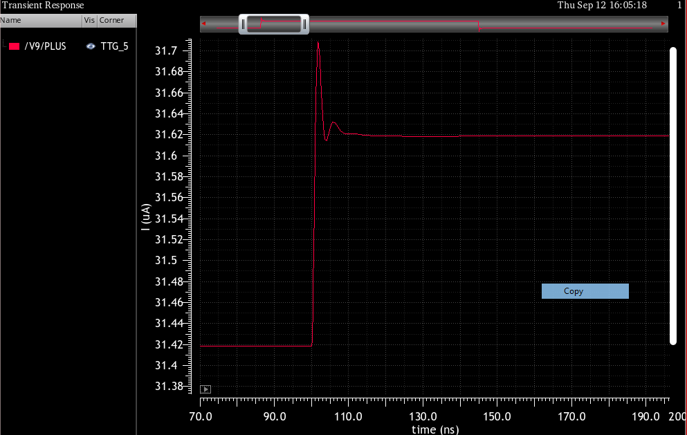
The transient step response looks like this:
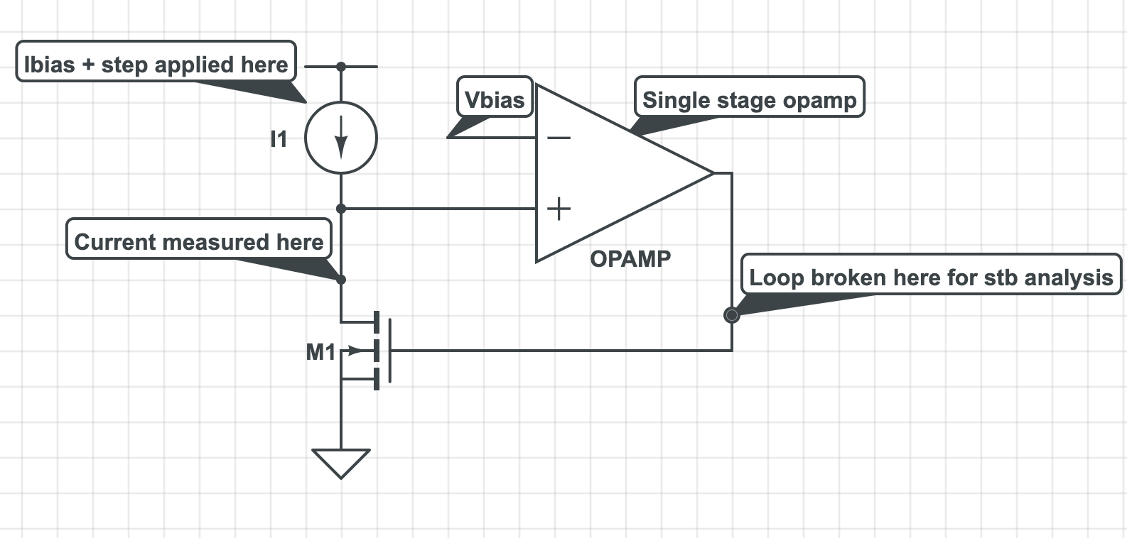
The block diagram looks something like this - basically a single stage op-amp (OPAMP in figure) with high gain (cascode structure) biasing a FET (M1) such that its drain is equal to Vbias.
A small signal step is applied at I1 Ibias and transient current through FET M1's drain is observed.
Am I missing something here?


