11
\$\begingroup\$

I've seen quite a lot of PCBs which have the passive components outlined all the way in their silkscreen.

Something like this:

enter image description here

Here there is an outline around each passive which goes (almost) all the way around, and seems to be sized exactly the same as the courtyard - the lines for components placed side by side overlap.

This style is apparently very common in high-volume stuff designed and mass produced in China - in this case a Bluetooth module, but I've seen lots of other boards which are the same.

Why is the silkscreen done in this way?

Is there a functional reason for it? Is there some way it makes assembly or inspection easier at volume?

\$\endgroup\$

5 Answers 5

24
\$\begingroup\$

Picture the workflow for initial prototypes on a long string of resistors like on that board. If not for the outline, you'd be forced to start at one end and proceed to the other, or risk getting off by half a component.

\$\endgroup\$
6
  • 19
    \$\begingroup\$ If you have a lot of close-packed parts and didn't provide outlines on the silkscreen, it might not even be clear if the parts should be installed horizontally or vertically. \$\endgroup\$
    – The Photon
    Commented Oct 22, 2019 at 17:29
  • 4
    \$\begingroup\$ Any polarity-sensitive components can also be marked with their polarity as part of this. \$\endgroup\$
    – Hearth
    Commented Oct 22, 2019 at 17:34
  • 2
    \$\begingroup\$ Hopefully the stuff you get to buy are not human-assembled initial prototypes. \$\endgroup\$ Commented Oct 23, 2019 at 7:23
  • 8
    \$\begingroup\$ @DmitryGrigoryev probably not, as robots are cheaper than slave labor, but hand assembly is probably part of the project history, and changing the screen after prototyping is a chance for errors to creep in. FAIK, the screen might be an aid for the pick and place programmers, as well. \$\endgroup\$ Commented Oct 23, 2019 at 10:47
  • 5
    \$\begingroup\$ @DmitryGrigoryev -- I mean visual inspection to make sure it's right. Sometimes it takes a few boards to tweak things out. My fabricators always plan on (worst case) losing a few at the start of a run, if things go wrong. \$\endgroup\$ Commented Oct 23, 2019 at 12:37
18
\$\begingroup\$

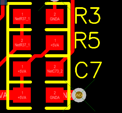
I do this all the time, the main reason being it allows a nicer visual appearance. The other nice thing about it is it enables a PCB designer to space components with minimum width between them.

Space can be a major factor on many PCB designs, nothing the minimum width can dance space (and make the design smaller)

enter image description here

\$\endgroup\$
2
  • \$\begingroup\$ Exactly. It's not just good for whoever has to pick'n'place/repair the boards, it's also helpful for whoever draws the thing. Visual references with known width you can see both on your screen and on the board itself while not being electrically relevant. \$\endgroup\$
    – Mast
    Commented Oct 24, 2019 at 8:19
  • \$\begingroup\$ One thing that is relevant is PCB space, which is a factor for many PCB designs \$\endgroup\$
    – Voltage Spike
    Commented Oct 24, 2019 at 13:28
13
\$\begingroup\$

Makes visual inspection of correct component placement easier to spot. Or to identify missing components. For example, I see two sets of pads with no components installed.

\$\endgroup\$
9
\$\begingroup\$

Silkscreen borders make the PCB layout easily readable by humans. They are not useful for automated PCB population or AOI.

Modules for electronics enthusiasts need to have readable PCB layouts because a lot of eyes will be looking at those PCBs. Mass-produced PCBs in finished products which are not intended to be serviceable often have little silkscreen, sometimes only identification codes.

\$\endgroup\$
2
  • 2
    \$\begingroup\$ Sometimes if assembler is working off pure Gerber's and not ODB or CAD data, they could use silkscreen info to manually configure the AOI and SMT equipment. \$\endgroup\$
    – crasic
    Commented Oct 23, 2019 at 14:53
  • 1
    \$\begingroup\$ @crasic Yes, but this doesn't require you to put physical silkscreen on the board during production. \$\endgroup\$ Commented Oct 24, 2019 at 9:03
8
\$\begingroup\$

The courtyard and the silkscreen are different things. The silkscreen is visible on the board, the courtyard is a design concept and visible only in the PCB Design Application.

Generally the silkscreen outline is slightly smaller than the courtyard outline. Courtyards can touch each other, so if the silk outline would be the same, two resistors would have a shared silk line if their courtyards touch. So the silk line must be a bit on the inside of the courtyard to make sure that there is some space between the silk lines of two different components as you see on boards.

The silk outlines and courtyards are suggested by the IPC-7351C document. In IPC-7351B the courtyards were rectangular, they can now be "arbitrary" and more closely follow the component's outline. The silk outline for resistors, diodes and capacitors are not rectangular either.

Below you can see a detail of one of my boards. I haven't updated the outlines of all my components yet - the lines in blue are the silkscreen lines, the lines in grey are the courtyards. You can confirm that this is inline with my explications above.

Board detail showing courtyards and silkscreen


Ben Voigt's remark caused me to look in more detail. The picture has some cases where the shared lines are larger (around the crystal) and other cases where the lines are smaller (between the columns on the far right). So it seems that the designer may have done one or more of the following:

  • Not use courtyards and only had silk lines, using them as some kind of courtyard;
  • Not respect design rules if he did have actual courtyards.
  • Had overlapping "courtyards" (for the cases where the silk line are smaller) - and this resulted in the production files being automatically adjusted to avoid having silk on the pads (these adjustments may be made by the PCB design tool, and are in my experience also applied by the manufacturer).
\$\endgroup\$
2
  • 1
    \$\begingroup\$ "if the silk outline would be the same, two resistors would have a shared silk line" The question postulates that this is happening, and backs the claim up with a photo. \$\endgroup\$
    – Ben Voigt
    Commented Oct 23, 2019 at 20:43
  • \$\begingroup\$ @BenVoigt Ok, looking in more detail, the photo shows touching lines, where the line appear larger, and smaller lines, where the components are closer to each other. I initially had the impression that a lot of them were larger. Updating the anwser. \$\endgroup\$
    – le_top
    Commented Oct 23, 2019 at 22:47

Your Answer

By clicking “Post Your Answer”, you agree to our terms of service and acknowledge you have read our privacy policy.

Not the answer you're looking for? Browse other questions tagged or ask your own question.