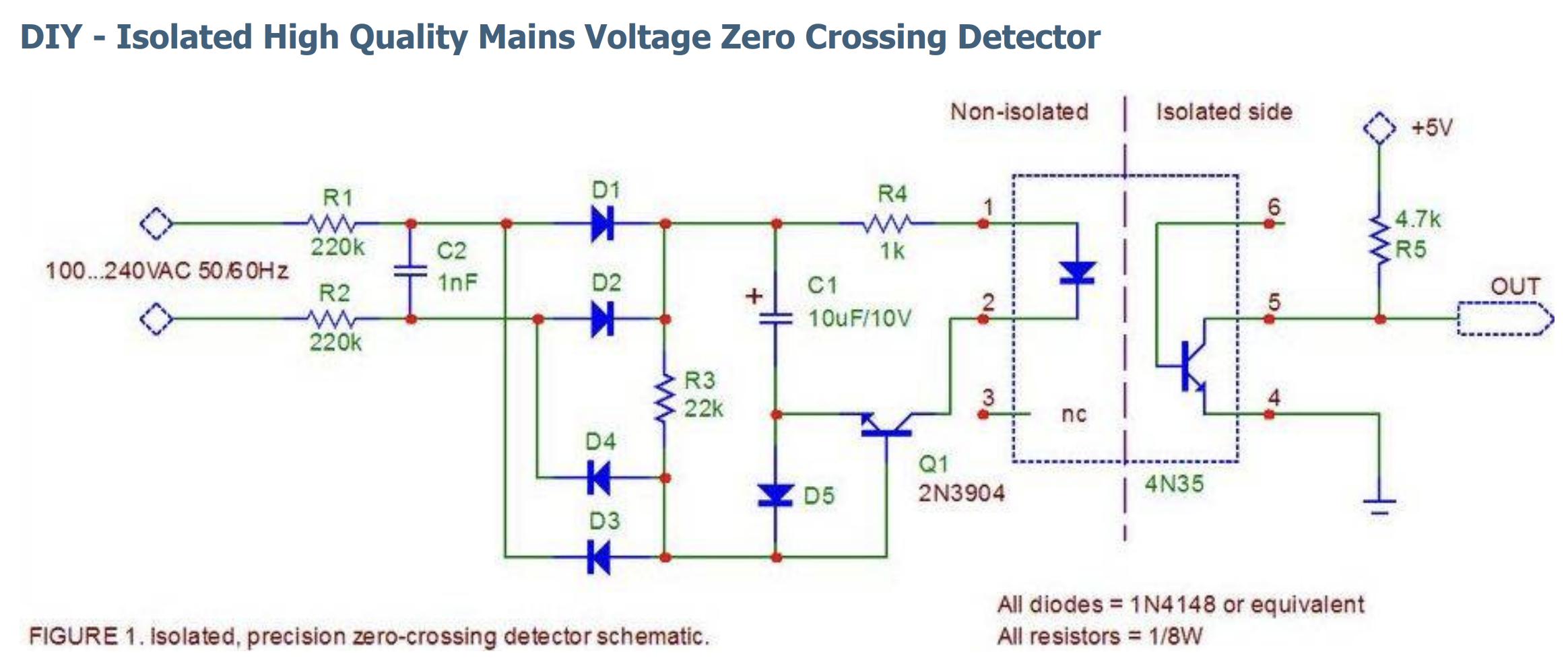
I'm considering using this zero-cross detector circuit in a design but I'm struggling to understand exactly how Q1 is activated. The description says "Q1 turns on and feeds current from C1 to the opto via R4, whenever the mains voltage (divided by (R1+R2)/R3) is lower than the voltage across C1." I understand this, but it doesn't explain how the base of Q1 is activated. In order for the optocoupler to indicate a zero crossing, the base must be activated only when a zero-crossing occurs, so its reasonable to assume that it has something to do with the capacitor discharging, but how it actually happens is still eluding me. Can anyone venture an answer?
4 Answers
D1-D4 form a bridge rectifier that will charge C1 up to about 1/20th of the peak voltage of the incoming AC power. (R1 + R2 are 440K, R3 is 22k 440/22 = 1/20).
During this time that C1 is charging the current will flow through C1 and through D5. This will reverse bias the base emitter junction of Q1 so it will not pass any current.
For a short period at the the end of each 1/2 cycle of the incoming AC the voltage will drop to a low value and C1 will start discharging into R3 via the base emitter junction of Q1. (The emitter will be negative with respect to the base). This in turn will cause a pulse of current to flow in the collector of Q1 through the optocoupler LED and R4 from C1 (which is still charged at this time).
The pulse of current will cause the output transistor of the opto-coupler to draw current and cause the output voltage to pulse to ground for a short time (500us-1ms).
These pulses will be centred on the zero-crossings of the input signal.
-
1\$\begingroup\$ These pulses are centered active low 500us before ZCS then high 500 us post ZCS \$\endgroup\$– D.A.S.Commented Nov 21, 2019 at 2:11
-
1\$\begingroup\$ @TonyStewartSunnyskyguyEE75 - thanks, that was what I was meant. \$\endgroup\$ Commented Nov 21, 2019 at 3:26
-
\$\begingroup\$ yes . and a higher 22k value like 50k reduces the PW so care must be taken if using edge-logic. \$\endgroup\$– D.A.S.Commented Nov 21, 2019 at 3:33
-
\$\begingroup\$ I elaborated on this in my answer below. \$\endgroup\$ Commented Nov 21, 2019 at 6:51
I am learning electronics myself and Kevin's answer confused me to the point where I was wondering what I was misunderstanding about the circuit, so I simulated it and found that my initial instincts and node analysis were actually correct. I will explain:
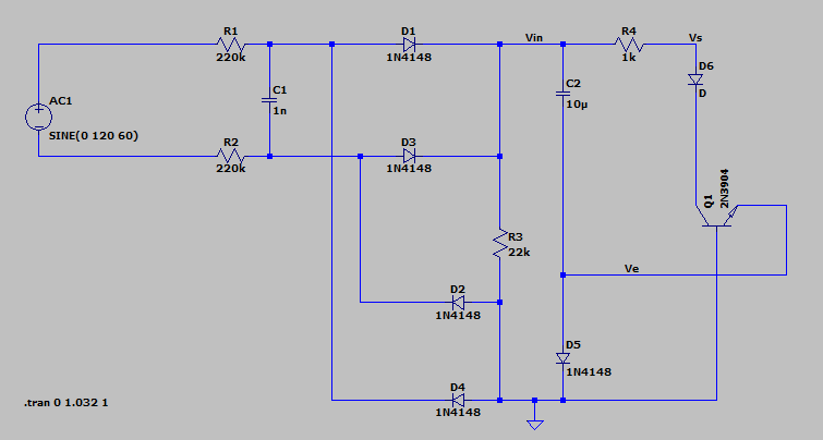
The following is my copy of your circuit in LTSpice, ignoring the isolation aspect, which should be straightforward, and is not what the question is about.
My understanding is as follows:
R1 and R2 serve primarily to limit the current from mains (120/240VAC).
C1 is a bypass capacitor that serves to smooth the input to the rest of the circuit.
D1 D2 D3 D4 form a full wave bridge rectifier. This normally functions to rectify an AC voltage source into DC, but in this circuit the values of the resistors and capacitors have been specially selected to perform a different function; zero cross detection.
R3 serves to control the voltage at Vin, the south end of this resistor can be thought of as ground.
C2 is a carefully chosen capacitor that would normally serve as the smoothing capacitor for the bridge rectifier, but in this circuit it's value in combination with resistor R4 control various properties of the zero crossing 'signal'.
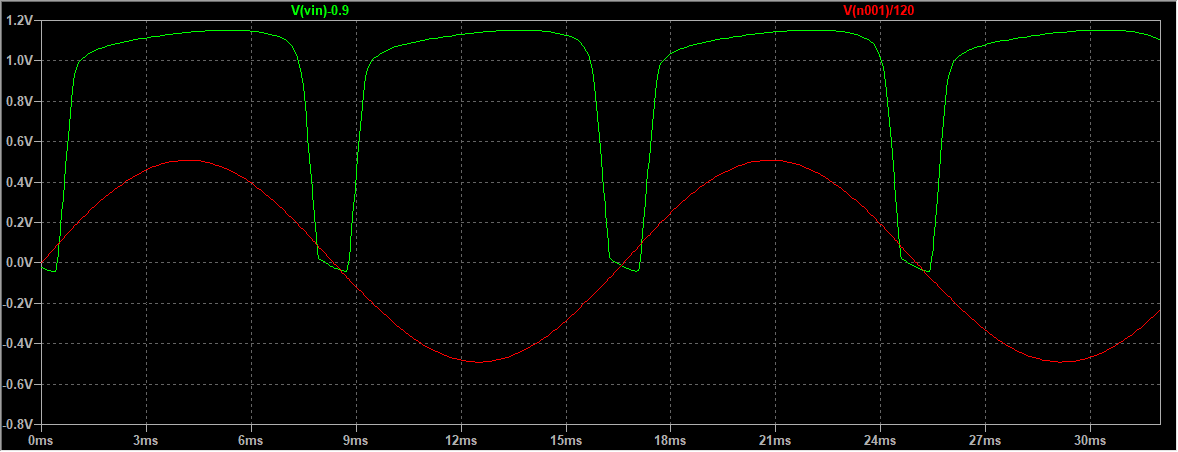
Here is the input signal and Vin superimposed. Note that when the input signal nears zero Vin is pulled low. This is the effect of the transistor going into its active region (explained below) and providing a path for the energy stored in the C2 to discharge through R4.
Note: I've done some math to superimpose Vin over the AC input signal so the output is clearer.
So the simulation seems to show the circuit functioning as desired.
How it works is a bit tricky, or at least I think so.
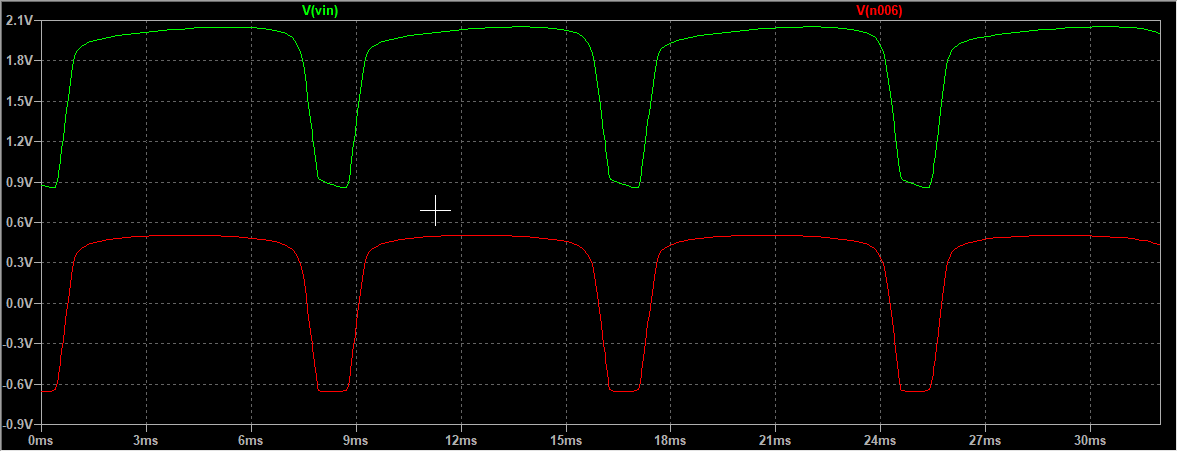
The following is Vin and Ve.
The effect of adding a diode at the cathode of C2 basically subtracts the peak voltage and then adds the diode voltage drop.
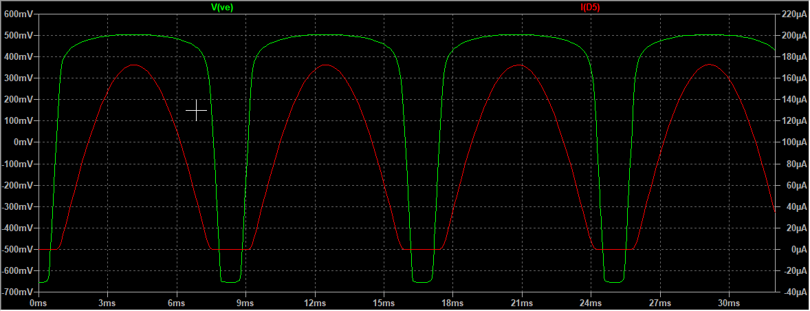
Note that Ve can actually go negative. This is the key to understanding the behavior of this circuit.
The following is a plot of Ve and the current through D5.
When Ve is going positive it hits a ceiling of 500mv or so. This is because 0.5V is the voltage in which the diode is forward biased and acts as a low resistance path to to ground. The voltage at Ve will remain at 0.5V because the capacitor is charged.
Because Ve can go negative in reference to ground and the base of Q1 is ground, Vbe of Q1 is positive which as we know will put the transistor into its active region and allow current to flow from Vc and Vb to Ve.
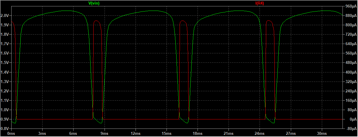
As the AC input nears zero C2 will drain through R3 until the voltage at Ve reaches -0.7V, and Q1 will become active as now Vbe is 0.7V. This creates a low impedance path for the remaining energy in C2 and the rest of the low input current to flow through R4 and the optocoupler (in your circuit).
This low resistance path is only available until the voltage at Vin rises to the point where the capacitor recharges and cuts off the transistor.
Here's a plot of Vin and the current through R4
-
1\$\begingroup\$ Couple of notes: The AC source value of Vp needs to be 170V to simulate an actual 120VACrms line voltage. Also R3 could be raised to 470K if you want the leading edge of the LED current pulse to be very close to the actual zero crossing instead of having the pulse centered at the zero crossing. In this case the C2 needs a voltage rating of 16V or more. \$\endgroup\$ Commented Nov 21, 2019 at 11:29
-
\$\begingroup\$ @MichaelKaras Thanks for the input, i forgot about the line voltage discrepancy. As for R3, i was intending to simulate the circuit in the question, so i retained the 22k value, however i did notice that the pulse can be tighter to the zero crossing point by increasing the value of R3. There are also tweaks to R4 and C2 that can serve to the same effect. \$\endgroup\$ Commented Nov 21, 2019 at 20:15
Some more notes:
In order to keep power consumption as low as possible (for an application running 24/7), I increased R1 and R2 to 560 kOhms each, and R3 to 33 kOhms. I further increased R4 to 2k2, and for Q1 I used a BC517 Darlington type. As optocoupler, I used a 4N35, as recommended.
This worked quite well, but I also wanted to keep impulses short (for firing a triac, I did not want accept impulse width of 1 ms, which I expected to fire the triac too early). For this purpose, I inserted a 5V1 zener diode in the base line of the transistor, and in order to diminish leakage current through the zener diode (before 5V1 is reached), I added a 100 kOhm resistor between base and emitter of the BC517. This procedure reduced the impulse width to about 200 microseconds.
Then I controlled for the phase of the detected zerocross relative to the actual mains zerocross. I found that the impulse was not centered around the actual zerocross (as expected) but just started with zerocross. This means, the impulse comes with some delay. I suppose that the 1nF capacitor C2 (which was 820pF in my case, because I only had this one at hand) causes delay, which becomes more pronounced with my increased resistors. I did some calculations on this, which I do not paste in here, but they supported the idea that C2 tends to delay the impulse. I was fine with a detector with the detection impulse starting right with the actual zerocross.
I am sorry for not providing a circuit after all these changes, but I do not have the software for that. I wanted to share my experience because it includes (a) saving power, (b) decreasing impulse width, (c) delaying impulse onset.
-
\$\begingroup\$ For future historical reference, I verified your design choices and agree with most except two. \$\endgroup\$– D.A.S.Commented Oct 23, 2021 at 17:49
-
1\$\begingroup\$ I agree with; IncreasingR1/R2 which reduces Pwr 50% especially for 240V 50Hz from 1/4W. Some differences in PW50 of ZCS pulse exist between 120V/60Hz and 240/50Hz. R3 is OK and R4 is OK only if using a Darlington but in any case does not reduce Pwr at all, due to low duty cycle. So original is OK. However C2 = 1nF or less has no effect on ZCS being centred or lagging, but > 6n8 will lag on 60Hz 120V+560K(2) enough to start ZCS after 0Vac and shift with increasing values while duty cycle is 10%. tinyurl.com/yhubcfvm \$\endgroup\$– D.A.S.Commented Oct 23, 2021 at 17:58
-
\$\begingroup\$ However C2 < 5nF lightly reduces PW50 pulse width with value of ZCS output negative pulse, yet not enough to call it precise. \$\endgroup\$– D.A.S.Commented Oct 23, 2021 at 18:17
-
1\$\begingroup\$ I once designed a simple offline ZCS using an XOR Gate for an 8 Channel Triac 1kW lamp sequencer chaser back in the 70's that looked somthing like this with 1% duty cycle 1% after the ZCS for adequate Triac gate current yet very close to 0V. I used a tiny pulse transformer to trigger the Triacs rather than RC. using this ZCS to enable a sequencer. tinyurl.com/ydossxve \$\endgroup\$– D.A.S.Commented Oct 23, 2021 at 19:27
Thanks to the answer of @Kevin White I understood it. The originally shown schematic is IMHO very difficult to understand. I added a schematic that should be easier understandable, because it shows better the current flow during zero crossing through R3, D7 and BE of npn darlington transistor, powered by the charge of C1. I used the input of @Wolfgang's improvements in the schematic.
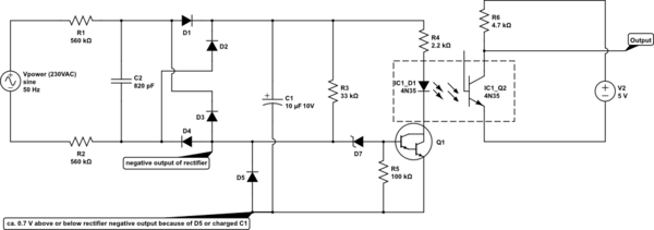
simulate this circuit – Schematic created using CircuitLab

