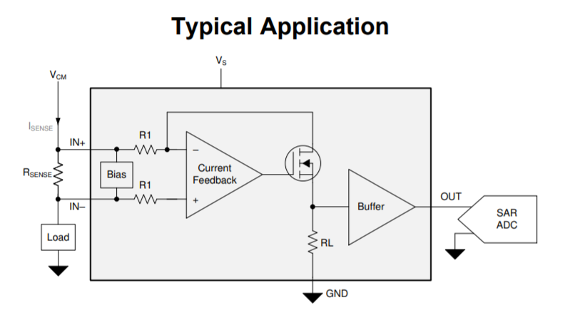
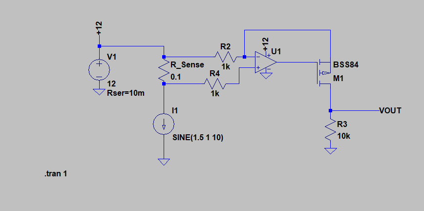
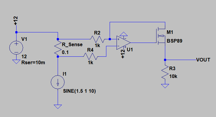
This is a fairly common high-side current sense amplifier topology.
There appears to be an error in the block diagram shown in TI's datasheet - as drawn, I don't believe it will work. Either the inputs to the current feedback amplifier are swapped, or they meant to draw a P-channel FET rather than an N-channel.
Let's look at this using the typical P-channel topology with a voltage-feedback opamp, since I find it the easiest to understand.

Here's how it works:
- There is a high-side resistor in series with the load (\$R_{sense}\$). Current consumed by the load causes a small drop across this resistor proportional to the load current.
- Without any action from the opamp or the transistor, the \$V_-\$ terminal will be at a slightly higher voltage than the \$V_+\$ terminal.
- The opamp will drive the gate of the P-channel FET down, allowing the P-channel FET to conduct.
- Feedback action adjusts the gate bias of the MOSFET so it is drawing enough current such that the drop across \$R_2\$ is enough to bring \$V_- = V_+\$. Since we know \$V(R_{sense}) = V(R_2)\$, we can state via Ohm's law that \$I(R_2)=\frac{I_{load}R_{sense}}{R_2}\$.
- For a voltage feedback op-amp, the \$V_-\$ pin is high impedance, so the only place for the current to go is through the transistor and through \$R_3\$. For a current feedback opamp this is also true, since the current feedback action nulls out the input current.
- Since the current we found earlier passes through \$R_3\$, we can state that the output voltage is the drop on \$R_3\$. That is: \$V_{out} = \frac{I_{load}R_{sense}R_3}{R_2}\$.
Note that since the output looks like a current source in parallel with \$R_3\$, this current sense amplifier has an output impedance equal to \$R_3\$. That's why you'll often see this circuit followed by a buffer amplifier.
You may also be wondering about \$R_4\$. It is for bias current cancellation and has the same value as \$R_3\$. If you're using an opamp with low input bias current, it can be left out and the \$V_+\$ terminal just connected directly to the low side of the sense resistor.
We've looked at the P-channel version, but this circuit works just as well with an N-channel device. For the N-channel version, swap the drain and source of the FET and swap the inputs to the opamp. One caveat with this configuration is you are limited to \$V_{out} < V_{supply} - V_{GS(on)}\$, but this generally is not an issue since you're usually interfacing with lower-voltage circuitry anyway.

Of course, you don't have to do this with FETs. PNP or NPN bipolar transistors work just as well.
The main advantage to this topology versus the typical differential opamp topology is there's no requirement for high performance or precision parts. You generally need precision matched resistors to get good common mode rejection with a differential amplifier, and good common mode is very important for a high-side amplifier since you are usually sensing with the largest common mode voltage anywhere in the circuit. You could go buy an instrumentation amp with nice on-die trimming, but that is more expensive. There are no precision resistors required in this design, and all the parts are cheap (opamp, transistor, a few commodity resistors). Resistor tolerance issues only affect your output accuracy, not your common mode rejection.
The main disadvantage to this design is that it is unidirectional: it only senses current in one direction. This is fine for the majority of use cases where you just want to measure the current going into the load. However, if you have an application where you need bidirectional sensing, such as measuring the current going both in to and out of a battery, you'd need a more complex solution.

