0
\$\begingroup\$

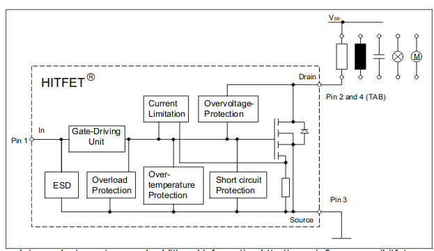
There are protected MOSFETs under various marketing names available (e.g. omnifet, hitfet, intellifet, etc). These devices include clamping diodes and overcurrent/temperature protection. They also seem to suggest that inductive loads can be connected directly:

Infineon-BSP78:
Datasheet

Imgur

AND8202:

ClampFET topologies utilize ESD protection at the gate input and active gate to drain clamping (described later), useful when switching inductive loads. [...] All topologies drive any type of resistive or inductive load such as solenoids, heater coils, and filament bulbs limited only by the current and thermal capability of the device

Usually flyback diodes are used directly across the inductive load (and not the MOSFET) to prevent voltage spikes if the transistor is turned off. Thanks to the overvoltage protection diodes the MOSFET should be safe, but other parts may not.

Should I use these protected MOSFETs without a flyback diode and what pitfalls may occur?

\$\endgroup\$
7
  • \$\begingroup\$ Leaving out the flyback diode is pretty much never recommended. \$\endgroup\$
    – Hearth
    Commented Dec 15, 2019 at 23:00
  • \$\begingroup\$ technically all mosfets are protected to some degree since they all have a parasitic diode, but it doesnt always work as well as it needs to. But the "protection" in the name of the device you have a diagram of doesnt mean protected from everything. Note the lack of a voltage protection block anywhere. it probably is referring to the oveccurrent and overthermal protections and variants, not inductive flyback. \$\endgroup\$
    – DKNguyen
    Commented Dec 15, 2019 at 23:48
  • 1
    \$\begingroup\$ Without a flyback diode, the device has to dissipate the energy from the inductor. With one the energy is dissipated either in the inductor or the snubber network. It can also be more efficient with an external diode although it may slow the release speed of relays. \$\endgroup\$ Commented Dec 15, 2019 at 23:48
  • 1
    \$\begingroup\$ @DKNguyen - the parasitic diode is in the wrong place to do anything useful for flyback as it will be reverse biased. If there is capacitance across the inductor such that it can resonate through a half-cycle it may end up conducting (as in line output stages for CRT deflection). \$\endgroup\$ Commented Dec 15, 2019 at 23:51
  • \$\begingroup\$ @KevinWhite yeah for non bridge schemes. \$\endgroup\$
    – DKNguyen
    Commented Dec 15, 2019 at 23:52

4 Answers 4

2
\$\begingroup\$

I opened a 60V part datasheet from Infineon BTS 117.

In the datasheet page 4, there is a section on Protection Functions, telling a single energy discharge the part can take (temp. dependent, of course). Footnote 2 says protection functions are not for repetitive operation. This is a clear statement you should not use this part without a flyback diode.

Further in the document, you may find the schematic of the protection circuit - zener diode from drain to gate. This will protect the part but it is stressed significantly more than the flyback diode would ever be, plus the gate driver inside needs to sink the clamped current.

Depending on your application, you may or may not be able to get away without the flyback diode. Without knowing the details I will say use the flyback diode.

Also, hear rules of thumb but don't always heed them. They exist for good reasons, but know the reasons to determine if they apply to you.

\$\endgroup\$
1
\$\begingroup\$

Additional protection is probably not needed in many cases. Adding more seldom hurts.

IF the OnSemi application note that you cite is applicable to the Infineon device that you cite (YMMV) and if the device has the same design criteria, then the information on pages 8 & 9 of the application note provide significant reassurance that you can abuse the device immensely without damage - the limit being (they say) being die heating 'in the normal manner'. In the OnSemi devices active protection is achieved by turning on the main switch when avalanche conditions are approached, but not reached. This results in energy dissipation in the switch in a(n apparently well enough) controlled manner. Again, YMMV with a device not covered by the application note.

Translation: The device does a very good job of protecting itself against anything half sensible you throw at it. There ARE limits - thermal design in the situation concerned is a major requirement.

FWIW: I used similar devices 20+ years ago.
I wondered about their response to to very high current faults.
I connected one across a car battery with thick short leads and operated it repeatedly. No problems! It functioned perfectly subsequently in normal use. Impressive.

AND8202/D: Low-Side Self-Protected MOSFET

They say:

"Fully protected low-side topologies incorporate all ClampFET features and add current limitation and overtemperature shutdown circuits. All topologies drive any type of resistive or inductive load such as solenoids, heater coils, and filament bulbs limited only by the current and thermal capability of the device. ...

There is a non fault operation mode where the overtemperature protection is not active and device failure is possible. When switching off an inductive load, the device must absorb the energy stored in the load inductor, equal to 1/2 (Li2). For standard MOSFETs, this operation mode is known as Unclamped Inductive Switching (UIS). ...

This failure mode is the same for the HDPlus low-side family of products, except these products use an active self-clamping technique from gate to drain to clamp the drain voltage below the avalanche breakdown voltage of the device. Active clamping will be explained in the next section, but essentially this technique, when used while turning off an inductive load, is known as self-clamped inductive switching (SCIS). The SCIS technique allows more energy to be absorbed by a device than a comparable device without active gate to drain clamping. However, there is a limit to how much energy the part can absorb, again limited by when the junction temperature exceeds the intrinsic temperature of the silicon. The point to realize is that during the SCIS event, the gate voltage is by definition at ground potential. Thus the control circuitry for the device is not biased and therefore the overtemperature limit circuit is not functional. The maximum energy rating for each device must be observed when switching inductive loads or it is possible to experience device failure due to the die junction temperature exceeding the intrinsic temperature. In addition, even if the maximum energy rating is observed, sufficient time between SCIS pulses must be allowed so that the junction temperature can cool down back to the initial starting junction temperature. Otherwise, the junction temperature can ratchet up after each SCIS cycle, eventually reaching the intrinsic failure temperature."

\$\endgroup\$
0
\$\begingroup\$

The "protection" in the name of the device you have a diagram of does not mean protected from everything. Note the conspicuous lack of a voltage protection block anywhere. It is only referring to the oveccurrent and overthermal protections, not inductive flyback or overvoltage across the MOSFET in general. Marketing.

\$\endgroup\$
0
\$\begingroup\$

Switches are inverting from Gate to Drain relative to the common Source.

FET body diodes are reverse biased in normal operation.
When an inductive load is switched OFF the drain voltage always changes in a direction such that the Body Diode remains reverse biased, so it cannot be protected without a flyback diode. This is consistent for both Pch and Nch.

The overvoltage protection sited is only a Zener from Drain to Gate of limited capacity.

It would protect for a Source Follower switch of an inductive load , but that mode is rarely practical.

\$\endgroup\$
4
  • \$\begingroup\$ Tony - you are almost always right or very right. This does not appear to be one of those times. On an eg N Channel device the load polarity reverses (which may be the basis of your comment) but the drain voltage rises, with the same polarity. Yes? \$\endgroup\$
    – Russell McMahon
    Commented Dec 16, 2019 at 1:42
  • \$\begingroup\$ Same polarity as Drain supply but opposite to direction of source where the body diode is connected. Drain would have to be negative or below NFET source to conduct body diode. Fix my wording if unclear \$\endgroup\$
    – D.A.S.
    Commented Dec 16, 2019 at 1:49
  • 1
    \$\begingroup\$ Agh - what you said is correct enough(of course :-) ) when read for total content and intention. I may change a few words - this does not change the core of what you said but removes the impression I gained. \$\endgroup\$
    – Russell McMahon
    Commented Dec 16, 2019 at 2:02
  • \$\begingroup\$ Interest only: The devices in the App Note he cotes (and maybe the actual parts he is looking at) are designed to turn on under inductive spike. Thermal limits under repeat inductive clamping set an upper limit to what can be achieved (as would be expected). \$\endgroup\$
    – Russell McMahon
    Commented Dec 16, 2019 at 2:05

Your Answer

By clicking “Post Your Answer”, you agree to our terms of service and acknowledge you have read our privacy policy.

Not the answer you're looking for? Browse other questions tagged or ask your own question.