0
\$\begingroup\$

I am going through this datasheet of a photo-transistor from Fairchild Semiconductor.

Problem-1: I cant figure out the gain of the photo-transistor (like in other normal BJTs). There is something mentioned Current Transfer Ratio which I guess has something to do with the gain of transistor. Not sure though.

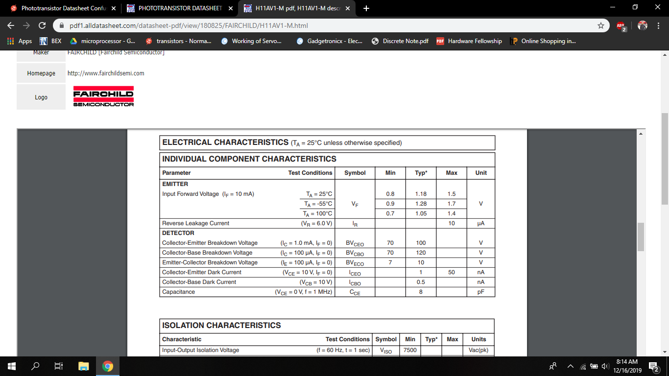
Problem-2: Why does the manufacturer mention two different values for "Collector- Emitter Breakdown Voltage" and "Emitter-Collector breakdown Voltage"? If one says 100V, should't the other say -100V? If the collector is forced 105 V with respect to emitter, the breakdown occurs. This also means my emitter is at -105 V with respect to collector. So why not just the reversal in sign for these two parameters?

\$\endgroup\$
3
  • \$\begingroup\$ problem 2 ... the voltage is being reversed \$\endgroup\$
    – jsotola
    Commented Dec 16, 2019 at 2:51
  • 1
    \$\begingroup\$ The H11AV1 is an optocoupler (or opto-isolator) that uses an LED and a phototransistor - it is not just a phototransistor. The current transfer ratio is the ratio of the LED current to the phototransistor collector current. \$\endgroup\$ Commented Dec 16, 2019 at 3:02
  • \$\begingroup\$ This should correctly be called an opt-isolator, not a phototransistor. \$\endgroup\$ Commented Dec 16, 2019 at 3:03

2 Answers 2

1
\$\begingroup\$

Problem-2: Why does the manufacturer mention two different values for "Collector- Emitter Breakdown Voltage" and "Emitter-Collector breakdown Voltage"?

Because the transistor in the the opto-coupler is meant to primarily run with up to 100 volts on the collector with respect to the emitter. If you run it in reverse firstly you will get operational problems and secondly it can't be expected to survive a reverse voltage greater than 7 volts.

Problem-1: I cant figure out the gain of the photo-transistor (like in other normal BJTs). There is something mentioned Current Transfer Ratio which I guess has something to do with the gain of transistor. Not sure though.

Remember that this device is an opto-coupler so it has an emitter (LED) and a receiver (photo-transistor) therefore, its main use is in opto-isolating and, for opto-isolation, the potential user is interested in how many mA you have to drive the LED with to how many mA you get on the transistor. This is called the current transfer ratio (CTR) and is quoted at between 100% and 300% at 10 mA. Figure 2 also tells you that if you operate with a slightly lower LED current (6 mA) you might get about 10% more CTR.

Although the device has a base connection and you might have thought that the data sheet would give hFE for the photo-transistor, it doesn't (and most of them don't). The only hint at what happens when you connect a resistor from base to emitter is shown in figure 4 so, if you can do the math and reverse things around, you might be able to eventually work out what the photo-transistor hFE is.

\$\endgroup\$
1
\$\begingroup\$

1) H11AV1 has a current gain of 1 to 3 which is product of hFE and optical attenuation. This is relatively good for a PT. Most of the variation is due to LED and hFE tolerances known to often exceed 300%, unlike Photo Diodes which are every stable and repeatable.

2) BVceo varies with collector current

  • disregard typical and use the worst case 70V min value.

    • I think you understand the polarity but BVceo (70V min) is the reverse of BVeco ( 7V min) which a -ve collector voltage.
\$\endgroup\$

Your Answer

By clicking “Post Your Answer”, you agree to our terms of service and acknowledge you have read our privacy policy.

Not the answer you're looking for? Browse other questions tagged or ask your own question.