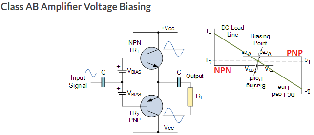
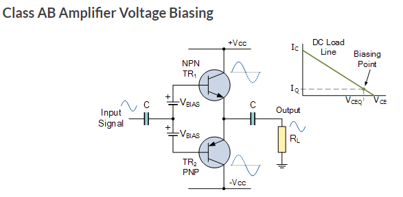
Class A biasing usually refers to a single transistor. Yes, Class A requires \$I_Q\$ to be about half-way. Class AB usually refers to two-transistor (push-pull), where one transistor takes care of upper half, while the other transistor takes care of lower half. Class B would set \$I_Q\$ at zero...Class AB offsets \$I_Q\$ with extra \$V_{BIAS}\$.
Your source diagram shows \$I_Q\$ for only one transistor (perhaps the NPN). A more complete load-line diagram might include biasing for both NPN & PNP transistor overlaid, as below. Note that with no Input signal the NPN+PNP transistors both are biased with \$I_Q\$ current flowing from +VCC through NPN collector-to-emitter, through PNP emitter-to-collector, to -VCC. This current establishes a linear load line through the zero signal point:

The NPN is supplying current to Output during the signal swings that are above the average. The PNP supplies current to Output during the signal swings that are below the average.
For the example circuit, a single polarity DC supply would work. But be aware that this is a somewhat conceptual, simple schematic, and wouldn't likely be seen in the real world.


