6
\$\begingroup\$

I'm trying to import an IC footprint into CAD software and can't seem to nail down the exact dimension for pin spacing. The two supporting documents seem to conflict with each other (Land Patterns here, and Package Drawings here).

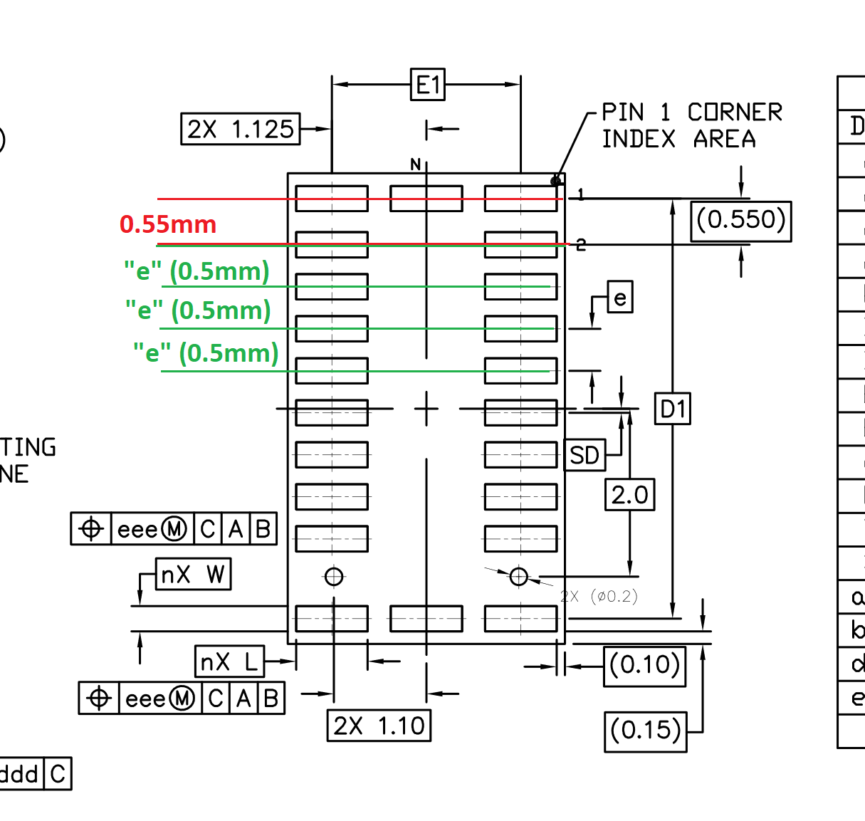
In the drawings document the pin spacing in the Y-axis is listed as 0.55mm whereas if you calculate the pin spacing from the land patterns it works out to be 0.50625mm (4.05mm/8 pins == 0.50625mm/pin).

If I try to go with the 0.55mm spacing the pins seem to be out of bounds of the package size and the spacing seem to contradict with the D1 dimension (5.0 BSC).

What is the correct dimension I need? And is BSC 0.55mm, 1.1mm or something else?

Curse you Maxim and your vague schematics! (Only their drawings, their technical specs are great)

\$\endgroup\$
0

1 Answer 1

8
\$\begingroup\$

I think the confusion lies in the 0.55mm measurement. This is not the pitch between every pin on each side of the IC, but rather the distance between the top row and the pins below.

The distance between the pins on each side is given by the measurement e, which is 0.5mm.

IC Pitch

I agree, this is a particularly confusing dimensional drawing.

\$\endgroup\$
2
  • 2
    \$\begingroup\$ I'd say that the dimensional package drawing is OK, but the land pattern is missing vital information available only in the package drawing. \$\endgroup\$
    – pipe
    May 26, 2020 at 14:23
  • \$\begingroup\$ That makes so much more sense now! Thank you, from me and my tired brain trying to work this out at the wee hours in the morning \$\endgroup\$
    – Tanenthor
    May 27, 2020 at 12:06

Your Answer

By clicking “Post Your Answer”, you agree to our terms of service and acknowledge you have read our privacy policy.

Not the answer you're looking for? Browse other questions tagged or ask your own question.