0
\$\begingroup\$

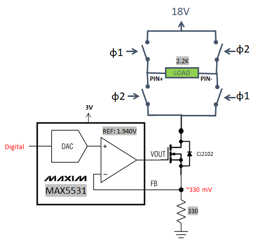
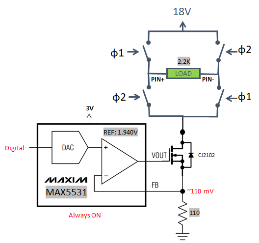
The circuit below shows a Voltage to Current converter based on a DAC, opamp, transistor and switches. The last one, allow to have a bipolar signal output.

enter image description here

During the experimentation, the DAC is setup to get ~330mV in the resistor (330 ohm) at the transistor source in order to get 1mA current and the LOAD.

The circuit (except the DAC) is simulate (in multisim) with success.

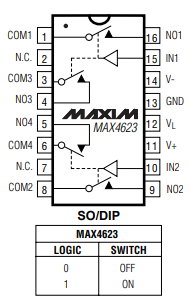
The switches used during experimentation are based on MAX4623.

enter image description here

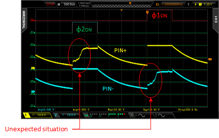
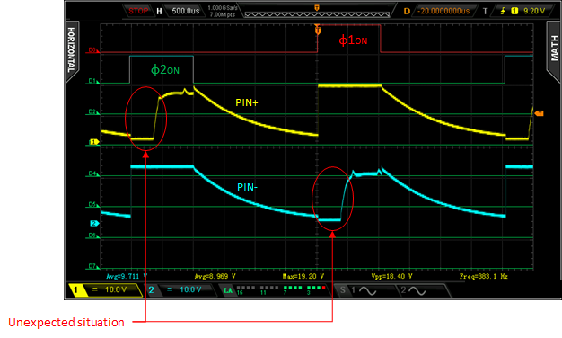
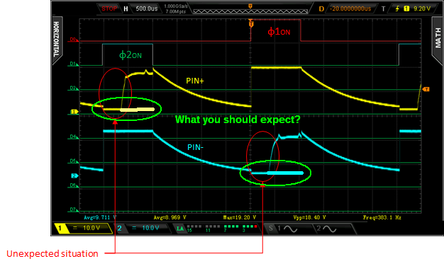
In the real world, there is an unexpected situation when the switch turn on (please, refer to the waveform below).

enter image description here

The waveforms of the LOAD (2.2K ohm) are shows in the scope chart (PIN+ and PIN-). Everything is as expected, except the part marked in red color.

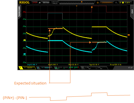
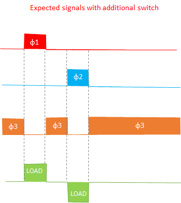
The expected waveforms are show below. These waveform allow to have a bipolar current (+/-) in the load.

enter image description here

Any suggestion in order to understand the unexpected situation is appreciated. As well as an approach to avoided.

Edit:

As suggested by Tony, the voltage in the mosfet source has been reduced to ~110mV.

enter image description here

The results in this experiment change a little a show the waveforms below:

enter image description here

Edit:

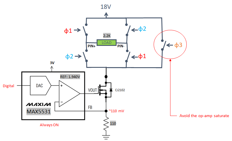
As suggested by Spehro, a switch could be added to avoid the op-amp to saturate.

enter image description here

Below the proposal and expected signals.

enter image description here

Edit:

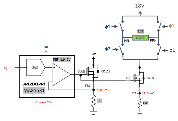
Below a proposal using a current mirror, following Tony and Spehro suggestions.

enter image description here

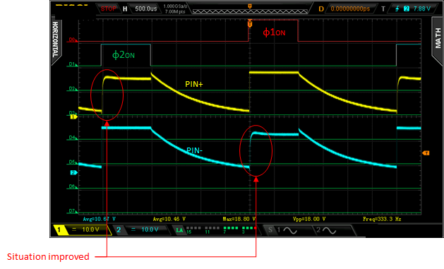
The waveform results improved with this proposal:

enter image description here

However, there are some not desired situations:

  • The left part of the mirror is always on, increasing the power consumption. Perhaps, a new question (based on this experimentation) will be: how to implement a ultra low power voltage-current converter (0 to 10mA)?
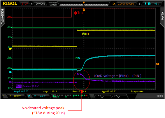
  • The initial peak (when the switch turn ON) is too high for the load. Please, refer to waveform below.

enter image description here

Edit (explain of unexpected situation):

As suggested, the unexpected situation is explained by the setting time of the op-amp. In summary, once the transistor turn on, the op-amp need time for adjustment (with the feedback). To solve this situation, the transistor is keep ON in order to allow the op-amp not saturated. One solution is presented in the proposal (see previous edit), where an additional transistor is added (making a mirror).

Thanks

\$\endgroup\$
4
  • \$\begingroup\$ You haven't shown your switch circuit. \$\endgroup\$
    – Andy aka
    Commented Jul 29, 2020 at 16:05
  • \$\begingroup\$ The switches used during experimentation are based on MAX4623 \$\endgroup\$
    – JACB
    Commented Jul 30, 2020 at 9:42
  • \$\begingroup\$ Why are you trying to accomplish a differential PWM current source? It has too many mismatched impedances. \$\endgroup\$
    – D.A.S.
    Commented Jul 30, 2020 at 12:19
  • \$\begingroup\$ I'm trying to accomplish a biphasic signal with fixed current (as show in the question) \$\endgroup\$
    – JACB
    Commented Jul 31, 2020 at 11:50

2 Answers 2

0
\$\begingroup\$

Assuming your timebase is 500us/div, consider that the settling time is listed at 660us typical and the slew rate as 10V/ms.

You may do better if you short the current source to +V during the 'off' periods so the op-amp does not saturate.

\$\endgroup\$
2
  • \$\begingroup\$ Hi Spehro, thanks for your feedback. As you mentioned, the unexpected situation seems related with the settling time of the DAC internal op-amps, which saturate when the mosfet is disconnected. In this case, I agree the solution proposed will improve the situation. I updated the images with this proposal. \$\endgroup\$
    – JACB
    Commented Jul 30, 2020 at 10:23
  • \$\begingroup\$ My concern with such proposal is the power consumption. I'm looking to reduce the power consumption as much as possible. In thi case, there will be a constant current from V+ to GND. The DAC is set one time (in order to reduce power) and the CPU controlling it, get to sleep. There is a custom circuit taking care of the switches signals. In other hand, another proposal could be keep the op-amp on and use a mirror as shown in the diagram (please, refer to the post edited). \$\endgroup\$
    – JACB
    Commented Jul 30, 2020 at 10:23
0
\$\begingroup\$

It is certainly unusual and suggests your high side analog switches are high impedance. Check that they have adequate gate voltage. Try CD4066's or similar for your experiment.

Reality is complex since the schematic does not show all the stray capacitance and protection diodes and unexpected results occur.

enter image description here

The switches complement the polarity of current to the load but then go to Tristate (unknown charge voltage) This does not seem practical and is neither a Sample and hold, nor a switch capacitor design, but something that does not behave properly with high impedance charges.

\$\endgroup\$
13
  • \$\begingroup\$ Tony, thanks for your comments. \$\endgroup\$
    – JACB
    Commented Jul 30, 2020 at 9:44
  • \$\begingroup\$ During the experimentation, the switches were based on MAX4623. The gate voltage level are compatible with the Logic Supply-Voltage Input (~3V). From your previous message, a new experiment was performed to reduce the voltage in the feedback around 100mV. In this case, the unexpected situation is still present, but a little different. Please, refer to the images in the post which I updated with latest experiment. \$\endgroup\$
    – JACB
    Commented Jul 30, 2020 at 10:23
  • \$\begingroup\$ This experiment has too many problems with complex high impedance, probe capacitance. Explain why you are doing it. \$\endgroup\$
    – D.A.S.
    Commented Jul 30, 2020 at 12:29
  • \$\begingroup\$ If you could measure switch voltage using two probes A-B, you may find more reasons why it fails. \$\endgroup\$
    – D.A.S.
    Commented Jul 30, 2020 at 12:40
  • \$\begingroup\$ Tony, please, may you list the problems that you consider with the circuit or experiment? The goal is to generate a biphasic signal in a variable resistive load (1k to 10k ohm) with a fixed current (0.1 to 3mA). The main constraint is to reduce the power consumption as much as possible. The biphasic signal is defined as below: !biphasic signal. \$\endgroup\$
    – JACB
    Commented Jul 31, 2020 at 12:01

Your Answer

By clicking “Post Your Answer”, you agree to our terms of service and acknowledge you have read our privacy policy.

Not the answer you're looking for? Browse other questions tagged or ask your own question.