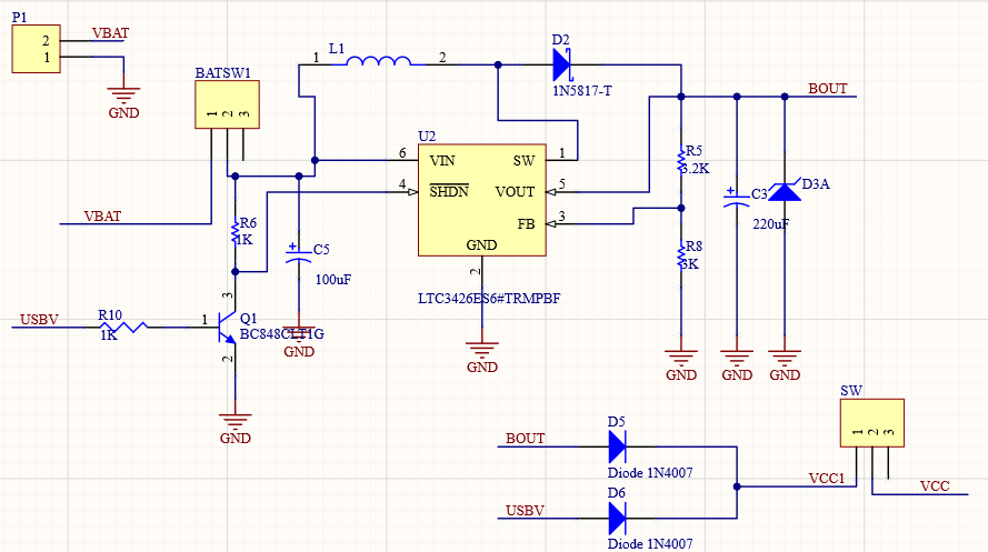
Here's the layout you posted:

Well... Don't take it personally, but it has all the mistakes we usually find in someone's first switching converter layout. You're not the first to get burned here ;)
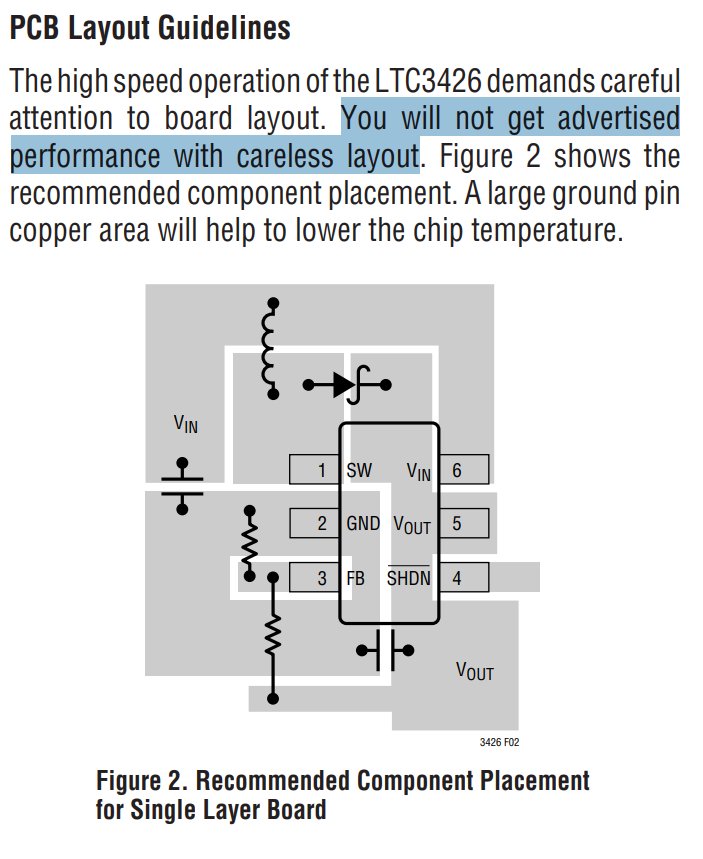
Layout is an essential part of any switching converter, especially a 1.2MHz one. From the datasheet:

So you have two solutions, depending on your goals.
If you just want it to work and need some 5V quickly, purchase a canned DC-DC converter like this one. These are readily available and cheap, and save a lot of time. You can still salvage your board if you mount it with very short wires, maybe recycling some thru hole pad (like the diode) to solder on.
If you want to learn about switching converter layout then it'll be a lot longer than what the $3.5 canned converter is worth. You'll also get some 5V, but only as a byproduct of the learning experience. If you intend to make a lot of boards then it'll also be worth the money versus a canned converter.
Problems with the layout:
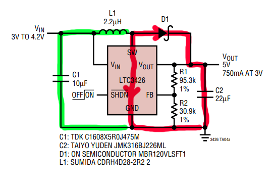
First, the hot loop (in red):

Depending on the state of the switch inside the chip, inductor current will flow in one of the two halves of the red loop. The switching has very high di/dt, a couple amps in a couple nanoseconds. Loop area is inductance (L) and problems are proportional to Ldi/dt, so you want L to be small thus the hot loop should have the smallest possible area. In your layout it is huge due to a thru-hole diode, long traces, no ground plane, and I don't see where the output caps are. Most likely this high inductance combined with high di/dt creates voltage spikes (ie, Ldi/dt) which fry your chip. So it won't work, and even if it did, another problem that is proportional to Ldi/dt is EMI emissions.
I'm not going to write a detailed guide, because it all boils down to: minimize the area of the hot loop (red) first, then the green loop second. You can find guides and tutorials, here is a good example.
So. You picked a non synchronous converter, which means it has an extra diode that has to fit somewhere. Honestly it's easier and simpler to use a synchronous boost like TPS61023, no diode, easier layout, and it has better efficiency.
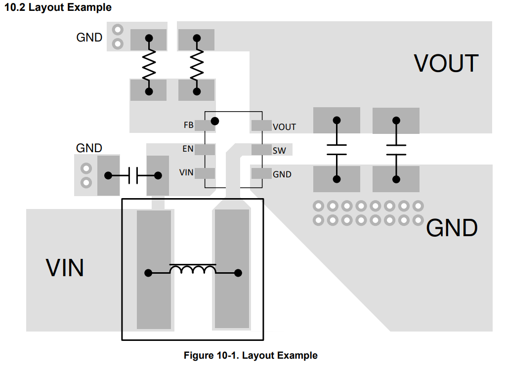
Optimizing the hot loop means a low inductance output cap, ie a SMD ceramic as close as possible to the chip:

There are vias for a low inductance connection to the ground plane too. This could be improved by moving the input cap in place of the inductor, so its ground pin connects directly to the output cap's ground, but this probably requires placing the inductor on the bottom side of the board.
EDIT:
Your layout looks like it was done with the autorouter. If this is the case, remember the autorouter has no idea what the traces actually do. It will happily route a 10 amp power rail for a motor with 0.3mm trace, and then the board will fry. It doesn't know decoupling capacitors have to be placed close to the load and routed tight. It will also tend to create long winding traces for power/ground and then it'll be happy that everything is connected together... but the extra impedance of these traces means you can get problems.
So it is important to think about placement, and put the components that need short traces where they should be. For example, a trace inductance of say 20nH is significant relative to a decoupling cap, to the point of making the decoupling cap useless but it is negligible when it's in series with a 1 kOhm resistor.
If placement is good, routing is usually easy. If routing gives you headaches, check the placement. For example I see a neat row of resistors on the screenshot, this looks nice but you get lots of hectic traces all over the place.

