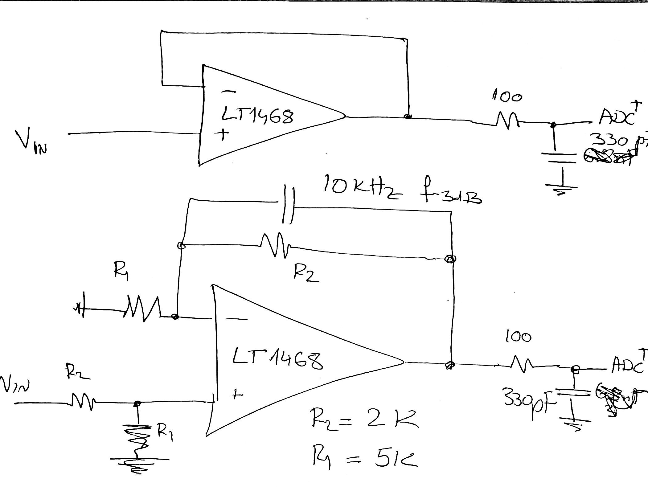
I am designing an ADC driver (20-bit differential ADC) with an input signal range from 0-10kHz, sampled at 1Msps and with 1 LSB of 47uV. I choose 1Msps rate for oversampling factor of 10.
Referring to my quick sketch (showing only one driver side for a bipolar ADC), the buffer configuration is obviously the simplest one, but the op-amp 90Mhz bandwidth means full bandwidth noise present on the op-amp output. However, with 5nV/sqrt(Hz) input noise op-amp, and using an additional RC filter on the ADC input (f-3db ~= 2.5Mhz) the total calculated noise is well under 1 LSB or about 12uV
In the second setup, with 10Khz LP filter the total calculated noise is <1uV. All components including the capacitor are matched to 0.1%
Do I really have the benefits of lower noise with the second setup or I just ask for more trouble with more components on the PCB around the op-amp with possible leakage currents and cross-talks with other traces running around, and not to mention that any mismatch among components will decrease CMRR of an ADC?

