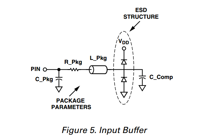
The main point of IBIS is to see how your digital ICs interface with analog circuitry external to those chips. Physical properties such as drive strength, pin leakage, and package parasitics can be vital in certain designs. IBIS is frequently used with PCB layout packages to validate signal integrity against the specifics of your copper traces, pours, substrates, etc. The main thing to understand about IBIS is its simplified input and output structures (see Analog Devices AN-715 AppNote), which are duplicated below (first image modified to fix position of package parameters):


One of the most useful applications of IBIS (in my opinion) is to use the V/T data of GPOs to calculate a Thevenin equivalent source resistance for the driver pin. Then you can easily plug a voltage source and resistor to interface with your remaining analog circuity in SPICE, or simply use that resistance value for hand calculations. There are tools/software e.g. SPISim_IBIS which can directly convert the IBIS I/V or V/T curves to behavioral SPICE curves, but it's slower and not as straightforward if you want to work out some things by hand. There's also a difference between ramp data and waveform data, and some free tools only let you use one of them.
I give an example below, so you can see for yourself. Something like this can be useful when interfacing digital outputs with gain circuits (think op amp or resistive DAC). You don't want to get burned by assuming an output pin's resistance is equivalent to 0Ω or something else. I prefer doing this calculation using my own lab measurements, but if I don't have hardware available (or I'm too lazy) I'll do it using the IBIS data.
STM32 microcontrollers seem to be popular lately from what I hear, so I'll use the stm32g030_031_041_so8n.ibs file found on ST's website. This is the file for the SO8N package version of the STM32G030. I'm going to work with the following model found in the file, which includes a description of the specific configuration for this type of I/O pin:
io6_ft_3v3_mediumspeed "GPIO-3.3V range - medium speed"
If you scroll or search for this model in the text, you will eventually see where it starts which looks like this:
|************************************************************************
|                    Model io6_ft_3v3_mediumspeed
|************************************************************************
|
[Model]  io6_ft_3v3_mediumspeed
Model_type I/O
Polarity       Non-Inverting
Enable        Active-Low
Vinl =   0.990000V
Vinh =   2.310000V
Vmeas =  1.650000V
Cref =   30.000000pF
Rref =   100.000000M
Vref =   0.0V
C_comp    1.290400pF        1.272500pF          1.305600pF
Scroll down a little further to where it says this:
[Rising Waveform]
R_fixture= 50.000000
V_fixture= 0.0
V_fixture_min= 0.0
V_fixture_max= 0.0
which means that this is Rising Waveform data when the output pin is connected to 0V via a 50Ω load. The idea is to analyze the ON state of the PMOS (top) transistor of the output structure.
If we scroll to the end of the time series data for that section we see something like this:
|time             V(typ)            V(min)              V(max)
|
...
...
...
29.949950nS       1.783884V         1.600996V           1.892836V
31.471471nS       1.788090V         1.602697V           1.901179V
31.631632nS       1.788290V         1.602898V           1.901984V
33.793794nS       1.791394V         1.605099V           1.910528V
34.914915nS       1.793096V         1.605499V           1.913845V
36.276276nS       1.794097V         1.605999V           1.917766V
39.879880nS       1.796100V         1.607300V           1.924400V
The last row is where they determined the output settled after fully switching from low to high. Another way to look at this is: when the pin is set high and you connect it to a 50Ω load to ground, there will be 1.796V (typically) at the pin. We can use the following formula to calculate the Thevenin equivalent resistance of the output pin:
$$
\begin{align*}
R_{\text{th(high)}} &= R_{\text{load}} \cdot \Big( \frac{V_{DD}}{V_{\text{load}}}-1 \Big) \\~\\
R_{\text{th(high)}} &= 50 \cdot \Big( \frac{3.3}{1.796}-1 \Big) \\~\\
R_{\text{th(high)}} &\approx 41.871 \Omega
\end{align*}
$$
If your external circuitry is only sensitive to when the pin is being driven high, then you should be fine with the above value. If not, then we can't assume the two transistors are exactly symmetric so let's do the same for the...
[Falling Waveform]
R_fixture= 50.000000
V_fixture= 3.300000
V_fixture_min= 3.000000
V_fixture_max= 3.600000
Notice how we're using the batch of values for when V_fixture is 3.3 V (there's another data set for 0 V, so be aware!). This means that the 50 Ω load is now connected to 3.3 V so we can analyze the ON state of the NMOS (bottom) transistor.
|time             V(typ)            V(min)              V(max)
|
...
...
...
29.789790nS       1.589774V         1.421969V           1.901713V
30.830831nS       1.586260V         1.418657V           1.898195V
31.551552nS       1.584452V         1.416348V           1.895882V
34.754755nS       1.577525V         1.409723V           1.887940V
35.075075nS       1.576922V         1.409121V           1.887438V
35.315315nS       1.576621V         1.408619V           1.886935V
39.879880nS       1.571300V         1.403500V           1.880300V
The formula is similar but slightly different (don't forget that exponent!):
$$
\begin{align*}
R_{\text{th(low)}} &= R_{\text{load}} \cdot \Big( \frac{V_{DD}}{V_{\text{load}}}-1 \Big)^{-1} \\~\\
R_{\text{th(low)}} &= 50 \cdot \Big( \frac{3.3}{1.571}-1 \Big)^{-1} \\~\\
R_{\text{th(low)}} &\approx 45.431 \Omega
\end{align*}
$$
You can use each resistance to build an output model using two voltage controlled switches with those two ON resistances, but a simpler approach would be to average the two resistances into one and use the result along with a simple independent voltage source:
$$
\begin{align*}
R_{\text{th(avg)}} &= \frac{R_{\text{th(high)}} + R_{\text{th(low)}}}{2} \\~\\
R_{\text{th(avg)}} &= \frac{41.871+45.431}{2} \\~\\
R_{\text{th(avg)}} &= 43.651 \Omega
\end{align*}
$$
One last caveat to point out is that usually the NMOS side has a lower resistance, and that didn't happen in this example. It could be because the time data ended without it fully settling to the final value...or it could be something else. This is one reason why I like doing my own measurements (calculations/formulas are the same), but hopefully this highlights a useful application of the IBIS model data.
The main downside to the above V/T curve method is that the R_fixture used for capturing the IBIS data might not even be close to what you are interfacing to the output pin. Furthermore, in the above example the 50Ω that was used puts the driving transistors in a region where their \$R_{DS(on)}\$ is quite non-linear. So using the 50Ω data in a situation where you're interfacing something closer to 470Ω will get you incorrect results. A way around this is to instead look at the I/V data for the approximate current you intend to drive using the device. Just like before, you can use this for only the PMOS using the [Pullup] data, only the NMOS using the [Pulldown] data, or averaging the results for both.
For this example (using the same IBIS model), let's aim for around 10mA and we'll look for "typical" values again. So we'll scroll to the [Pullup] data. IBIS convention is that positive currents flow into the component. Unless we're connecting our load to something higher than 3.3V we'll be sourcing current from the device and out of the pin. Therefore, we're looking for a negative current around 10mA.
[Pullup]
|Voltage   I(typ)              I(min)              I(max)
|
...
...
...
  -0.30    11.466000mA       11.979999mA         10.497975mA
  -0.20    7.604799mA        7.956100mA          6.973075mA
  -0.10    3.786300mA        3.967000mA          3.464625mA
  0.00    0.230000pA        0.0A                0.643000nA
  0.10    -3.671800mA       -3.824800mA         -3.370709mA
  0.20    -7.144100mA       -7.386300mA         -6.596109mA
  0.30    -10.421000mA      -10.692000mA        -9.677909mA     <=====
  0.40    -13.506000mA      -13.751000mA        -12.618008mA
  0.50    -16.404000mA      -16.568000mA        -15.418008mA
...
...
...
Skimming the data, I chose the line of data with the arrow pointing to it, which seems to have a typical current closest to our goal. Using the magnitudes of the voltage and current here along with Ohm's law gets us:
$$
R_{\text{th(high)}} = \frac{0.3 \text{V}}{10.421 \text{mA}} \approx 28.788 \Omega
$$
Doing the same for the Pulldown data, but looking for a positive current (sinking current; i.e. into the pin) gets us:
[Pulldown]
|Voltage   I(typ)              I(min)              I(max)
|
...
...
...
  -0.30    -10.656865mA      -11.865999mA        -8.724131mA
  -0.20    -7.110396mA       -7.918200mA         -5.825767mA
  -0.10    -3.558800mA       -3.963500mA         -2.915933mA
  0.00    20.000000fA       0.0A                0.0A
  0.10    3.478700mA        3.853300mA          2.862306mA
  0.20    6.788800mA        7.476800mA          5.610805mA
  0.30    9.930300mA        10.870000mA         8.245504mA     <=====
  0.40    12.903000mA       14.033000mA         10.766004mA
  0.50    15.707000mA       16.964000mA         13.173003mA
...
...
...
$$
R_{\text{th(low)}} = \frac{0.3 \text{V}}{9.9303 \text{mA}} \approx 30.211 \Omega
$$
And finally, averaging the resistances of each transistor into a single value yields us:
$$
\begin{align*}
R_{\text{th(avg)}} &= \frac{R_{\text{th(high)}} + R_{\text{th(low)}}}{2} \\~\\
R_{\text{th(avg)}} &= \frac{28.788+30.211}{2} \\~\\
R_{\text{th(avg)}} &\approx 29.500 \Omega
\end{align*}
$$


