0
\$\begingroup\$

A lot of literature on bus bar design suggests that bus bars should be made to overlap or have equal area such as this.

The reason they mention is the total stray inductance falls due to increase in mutual inductance.

Bus bars represented by parallel conducting plates:

Bus Bars represented by parallel conducting plates

If top plate represents the top DC bus and bottom plate represents the bottom DC bus, the total inductance according to the paper is:

$$ L_{tot} = 2 \times (L_{self} - L_{mutual}) $$

Where \$ L_{tot} = Total inductance of bus bar, \$

\$ L_{self} = Self inductance of bus bar, \$ \$ L_{mutual} = Mutual inductance between top and bottom plates \$

But if currents are flowing in opposite directions are, should the formula not be:

$$ L_{tot} = 2 \times (L_{self} + L_{mutual}) $$ by right hand thumb rule - but then increasing overlap area and increasing mutual inductance would not make sense, yet that is how most bus bars for inverters are engineered.

Can someone please tell me what is the correct explanation of this?

\$\endgroup\$
2
  • \$\begingroup\$ To minimize inductance. \$\endgroup\$
    – winny
    Commented Sep 14, 2021 at 7:33
  • \$\begingroup\$ I guess the equation already takes into account that currents flow in opposite directions, you can see it on depiction. \$\endgroup\$ Commented Sep 14, 2021 at 9:47

2 Answers 2

1
\$\begingroup\$

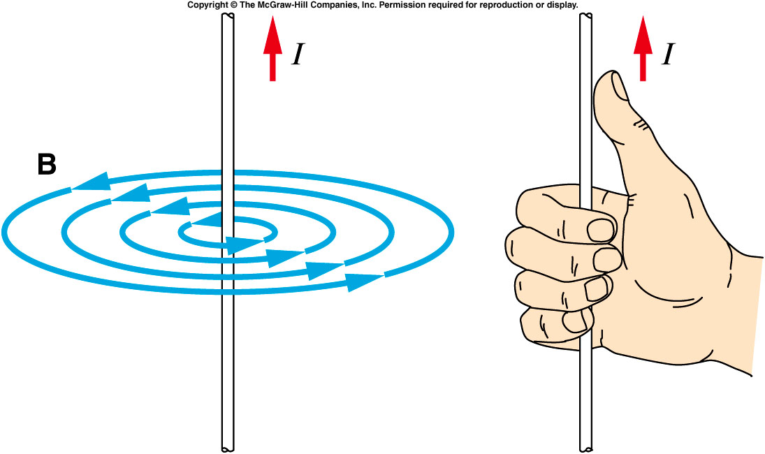
The magnetic field lines surrounding the upper plate with positive current flowing into the page will be flowing from left to right above the conductor and right to left below that conductor as per the right-hand rule below: -

enter image description here

Image from here.

The field lines due to current travelling in the opposite direction due to the current in the lower plate will cancel out those upper-plate field lines outside the insulation layer. This means the inductance is reduced and reduces more as the distance between upper plate and lower plate get closer.

\$\endgroup\$
3
  • \$\begingroup\$ Th field lines due to lower plate will also go from right to left. The would not cancel rather will aid the flux in the insulation region will increase and hence mutual inductance would also increase. \$\endgroup\$ Commented Sep 14, 2021 at 11:14
  • \$\begingroup\$ @SambeetPanigrahi oops a typo I meant to say outside the insulation layer and given that the overall external field is reduced the nett inductance also reduces. Yes they concentrate in the insulation layer. \$\endgroup\$
    – Andy aka
    Commented Sep 14, 2021 at 11:28
  • \$\begingroup\$ As the two plates come closer the leakage inductance reduces and the mutual inductance tends to be the value of the inductance of each plate. \$\endgroup\$
    – Andy aka
    Commented Sep 14, 2021 at 11:36
0
\$\begingroup\$

Self-inductance isn't very meaningful here, as a closed loop cannot be defined for a segment of conductor.

There is a closed loop between conductors, however: suppose we short one end of the pair, and inject current / apply EMF at the other end. Then we have a flat (broadside-parallel) hairpin loop, and the current path and inductance are easily recognized.

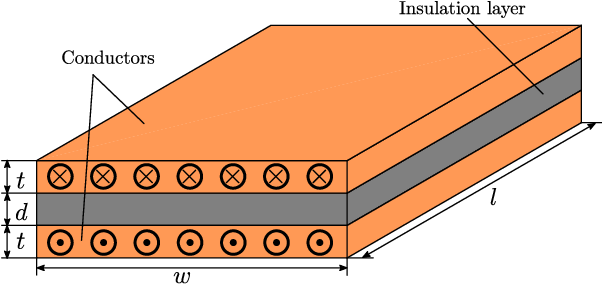
This gives a parallel plate transmission line structure, which can be understood as such:
Parallel-Plate Waveguide | LibreTexts Engineering

We have, $$ Z_0 = \eta \frac{d}{w} $$ where η is the impedance of free space (or for some magnetic or dielectric loading surrounding the plates, \$\sqrt{\frac{\mu_r}{\epsilon_r}}\$ times that), and d and w are the dimensions as pictured.

Specifically, this is for the wide-plate case \$w \gg d\$ where fringing can be ignored; for narrower plates or wider spacing, the field solution begins to resemble the parallel-wire case, and exact solutions are complicated.

The impedance, velocity factor \$c\$, reduce at low frequencies to give a series L and shunt C equivalent, \$L_0 = \frac{Z_0}{c}\$ and \$C_0 = \frac{1}{Z_0 c}\$ (in units of H/m, F/m; multiply by electrical length to get the in-circuit value).

We don't need to invoke full transmission line theory to arrive at an LF-equivalent value, of course, and can do the [magneto/electro]static problem just as simply. In short: it's basically dimensional analysis, with a leading coefficient of 1; rub together the right units and constants, and you get the right answer out.

Likewise, the reason this geometry is chosen, is to minimize inductance and maximize capacitance, for use in low-impedance circuits where these parameters should be optimized in this direction. The external field is also reduced, which can be important for reducing interference to nearby circuits; this applies even at low frequencies or DC, where the inductance is unimportant but the Lorentz force matters (reducing, or better distributing, forces upon the bus bars due to, say, 100kA peak mains fault currents, or in a 40kA aluminum smelting rectifier supply).

\$\endgroup\$

Your Answer

By clicking “Post Your Answer”, you agree to our terms of service and acknowledge you have read our privacy policy.

Not the answer you're looking for? Browse other questions tagged or ask your own question.