1
\$\begingroup\$

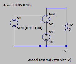
I've simulated the following circuit with the defined values for SW parameters as follows: (Vt=5 and Vh=-2).

enter image description here

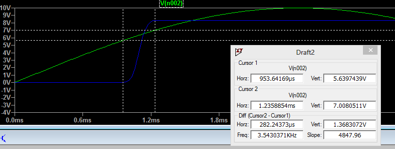
The resulted waveforms are not understandable for me. according to the following figures, for changing the status from off to on, the smooth transition starts from almost 5.5 V and ends in 7 V. I can't understand its relation to Vt-Vh and Vt+Vh.

enter image description here

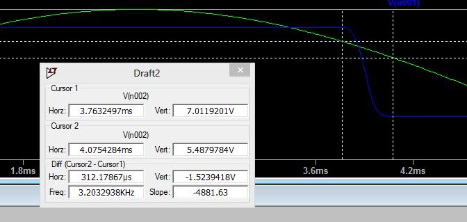
Also for changing the status from on to off, the smooth transition starts from almost 7 V and ends in 5.5 V. and I can't understand its relation to Vt-Vh and Vt+Vh.

enter image description here

\$\endgroup\$

2 Answers 2

2
\$\begingroup\$

Try to not judge "visually", because you can get deceived. In this case, the time when the VCSW starts conducting is (according to the manual, LTspice > Circuit Elements > S. ...):

If Vh is negative, the switch will smoothly transition between the on and off impedances. The transition occurs between the control voltages of Vt - Vh and Vt + Vh.

Therefore, given your settings, the conduction occurs between 3 V and 7 V. If you can't determine this visually it's because the defaults are Ron=1 and Roff=1/Gmin=1e12, and the midpoint is \$\sqrt{R_{on}R_{off}}\$, and the smaller values simply get buried in pixels. The resistance is, also according to the manual:

The smooth transition follows a low order polynomial fit to the logarithm of the switch's conduction.

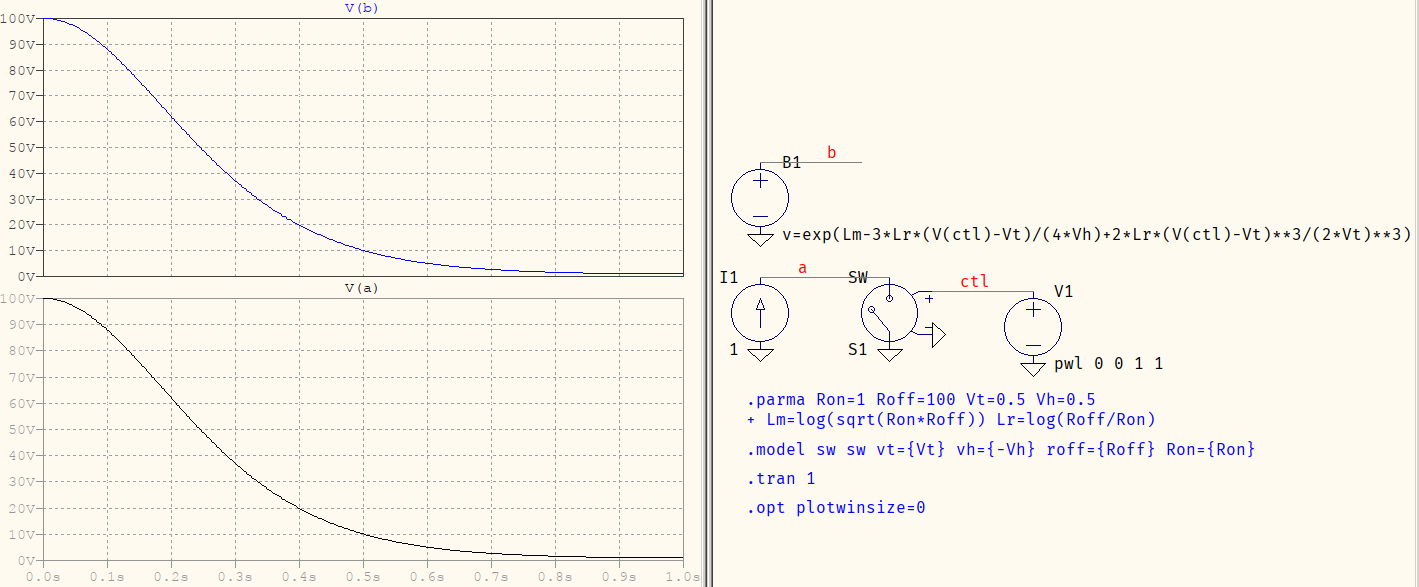
If you're really interested in details, the exact formula is:

$$\begin{align} R&=\exp{\left[R_{ls}-3R_{lr}\left(\dfrac{V_{ctl}-V_T}{4V_H}\right)+2R_{lr}\left(\dfrac{V_{ctl}-V_T}{2V_H}\right)^3\right]} \tag{1} \\ R_{ls}&=\log{\sqrt{R_{on}R_{off}}} \\ R_{lr}&=\log{\left(\dfrac{R_{off}}{R_{on}}\right)} \end{align}$$

This is for level=1, and you can also find it if you search for PSPCREF.PDF on the web (it's the manual for PSpice, it should be freely available). For level=2, the formula is described in LTspice's manual (same page).

Here's a test jig (and confirmation) for the above:
test

Don't forget that part of the confusion is the driving voltage for your schematic: a sine, versus a linear ramp, like in my example.

\$\endgroup\$
2
\$\begingroup\$

The switch starts to conduct when V3 reaches 3v (at about 0.5mS), it's just that you can't see the current on the display's linear scale!

Current I(R2) with the switch OFF is a few pA. When Vh is negative, I(R2) increases slowly to begin with only reaching 1microA at around 0.8mS.

I found the relevant info at http://ltwiki.org/index.php?title=S_Voltage_Controlled_Switch

The important part of the explanation is "If Vh is negative, ... The smooth transition follows a low order polynomial fit to the logarithm of the switch's conduction."

In order to check exactly what was happening, I recorded the simulation in ASCII files (in LTSpice XVII: Control Panel > Compression > ASCII data files > tick). To avoid huge output files, limit the simulation time to 2mS and increase the Maximum Timestep to 10u.

\$\endgroup\$

Your Answer

By clicking “Post Your Answer”, you agree to our terms of service and acknowledge you have read our privacy policy.

Not the answer you're looking for? Browse other questions tagged or ask your own question.