2
\$\begingroup\$

So here it is:

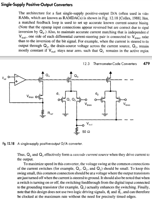
enter image description here

I don’t know how exactly this circuits works. I don’t understand how that feedback loop sets up an accurate know current source biasing, and what transistor is it trying to bias, Q4? For what?

With accurate current matching I presume it means that currents stay the same no matter what the voltage Vout is, but exactly what currents and why does this circuit need this? How does putting Vbias in one of the transistors in the pair differential helps this? I don’t understand.

Lets say I have code 10 as my input, so I presume d1 = 1 (or some other voltage) and d2 = 0. What happens next?

\$\endgroup\$
0

2 Answers 2

1
\$\begingroup\$

This architecture is based upon a simple current steering dac. Although, usually it allows for differential input signal control words (\$d_{1}\$,\$d_{1N}\$,\$d_{2}\$,\$d_{2N}\$,...\$d_{k}\$,\$d_{kN}\$) and a differential load (\$R_{L}\$ on each leg).

"I dont know how exactly this circuits works. I dont understand how that feedback loop sets up an accurate know current source biasing, and what transistor is it trying to bias, Q4? For what?"

An ideal current steering dac will have perfect current sources that add (across a resistive load) to create a voltage output proportional to switches turned on or off. So you would like close to ideal current mirroring under all conditions. The current source on the left mirror leg provides feedback and a high impedance cascode to help acheive this. It can usually be set by some Rref and vref that will fix the current of the mirror source and provide robustness against variations. The loads of the mirror are each of the current steering blocks. Forcing one to be fixed with vbias will help create ideal loads for the mirror and improve matching (rather than have the loads vary with differential inputs).

The switches \$d_{1}\$,\$d_{2}\$, to \$d_{k}\$ will simply steer current proportional to the input codes and sum across the output \$R_L\$=50 \$ohm\$. So for example, if you had \$d_{1}\$,\$d_{0}\$ = 1,0 you would get half \$I_{1}\$ plus a full \$I_{0}\$ or \$Vout= \$(\$I_{1}*\frac{1}{2} + I_{0}\$*1)\$*50ohm\$.

You might have an easier time starting with understanding a basic fully differential current steering dac.

edit* per request in comment, here is a good tutorial from Behzad Razavi. Note he doesn't show much in the way of current mirror architectures, but you can look up robust current mirror design for that.

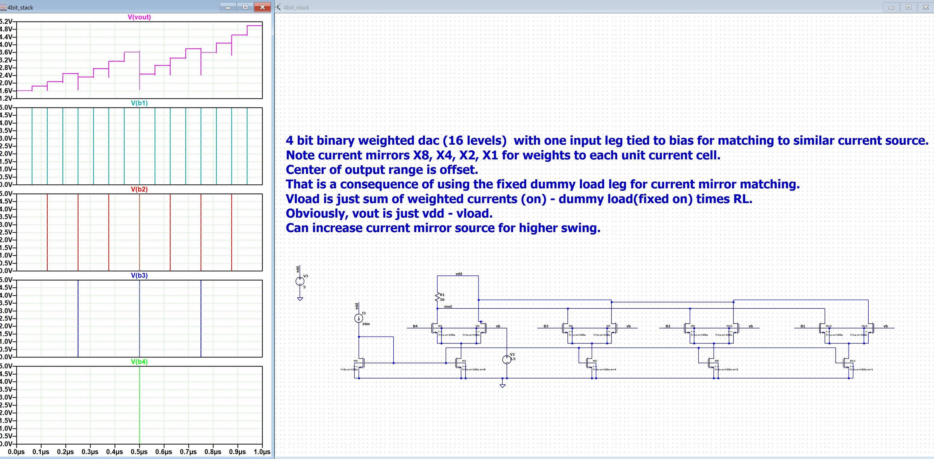
edit2* I built an lstpice simulation to help you further. It uses binary weighted current cells and nmos inputs. It should be fairly simple to translate to thermometer (X1 for each current cell weight). You can just flip upsidown and use PMOS to match book.
enter image description here

\$\endgroup\$
9
  • \$\begingroup\$ Do you have any good sources in this basic fully differential current steering dac? Cus i dont find anything usefull. \$\endgroup\$
    – Scipio
    Commented Apr 4, 2022 at 23:06
  • 1
    \$\begingroup\$ link added to post. \$\endgroup\$
    – pat
    Commented Apr 4, 2022 at 23:10
  • 1
    \$\begingroup\$ If the gate voltage on Q3 is the same as it is on Q4, then the current sourced by Q3 will be identical to that sourced by Q4. This applies to all the FETs to the right of Q4. And this relationship holds so long as the characteristics of all the FETs are identical. If that's not the case, then the currents will be different, even with the same gate voltage. \$\endgroup\$
    – SteveSh
    Commented Apr 4, 2022 at 23:58
  • 1
    \$\begingroup\$ @GotBlackOps. Q3 and Q4 have same S and G voltages, so same current. That is basic mirror (assuming load mirror does not vary too much). If a control switch is off all the current will flow to the load node via the fixed switch. If a switch is on, half will flow to load and half through the switch. \$\endgroup\$
    – pat
    Commented Apr 5, 2022 at 0:15
  • 1
    \$\begingroup\$ In this case we assume they are the same (thermometer coded). They could also be weighted as binary or another scheme. I highly suggest to build this in a simulator like ltspice. Use a very simple current mirror (two transistors) to understand the mechanisms. \$\endgroup\$
    – pat
    Commented Apr 5, 2022 at 19:08
1
\$\begingroup\$

When V(Rref) = Vref then I4 is known from Vref/Rref=I4 since the comparator nulls the input error with negative feedback using the 1st FET on the comparator as an inverter to the non-inverting feedback input for NFB.

This is common practice. The 2nd FET below it is a common gate config. and thus non-inverting, thus overall it is negative feedback (NFB).

\$\endgroup\$

Your Answer

By clicking “Post Your Answer”, you agree to our terms of service and acknowledge you have read our privacy policy.

Not the answer you're looking for? Browse other questions tagged or ask your own question.