3
\$\begingroup\$

enter image description here

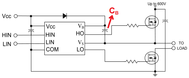
I have been trying to understand this circuit, but I just don't get how the boot strapping works.

Correct me if I am wrong but if I apply 400V at the drain of the high side MOSFET, the gate needs 410V to turn it on (assuming that this is a typical power MOSFET.)

Where does the high voltage needed to supply the gate come from? It can't be the capacitor because that's only charged to Vcc (say 10 volts.)

Does the 400V come from the VS pin? Does it combine with the voltage supplied to Vb (which comes from the capacitor) to produce 410 volts at HO, or is that wrong.

How would 400V even be supplied to the Vs pin? An explanation on how this works would be very helpful.

\$\endgroup\$
1

3 Answers 3

8
\$\begingroup\$

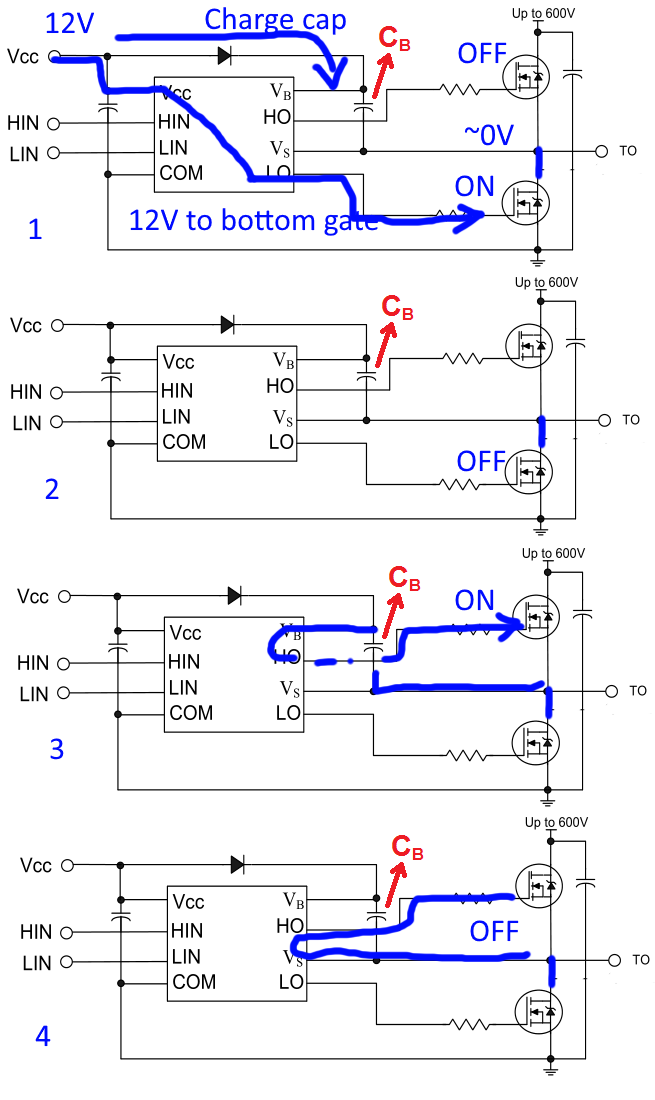
It won't work as shown on the schematic in your question. The two wires to the load have to be one wire. I've fixed it below:

enter image description here

  1. The driver turns on the bottom FET using its own +12V power supply. The bottom FET source is at GND, so a GND-referenced 12V supply will give it the Vgs it needs to turn on.

When the bottom FET conducts, the output node ("to load") drops close to 0V. Then, the bottom pin of the bootstrap cap, which is connected to it, also drops to 0V. Thus the cap charges from the +12V supply through the diode.

  1. The driver turns off the bottom FET by sending OV to its gate.

  2. The high side part of the driver is powered by the voltage on this capacitor, between pins Vb and Vs. It turns on the top FET by connecting its gate to the bootstrap cap's top pin Vb. Since the cap's bottom pin is connected to the top FET's source, this gives it close to 12V Vgs. It turns on, conducts, and its source voltage rises to the high voltage supply. The cap is still charged, so it rides along, its upper pin (Vb) sitting 12V above the high voltage supply, and it keeps powering the chip and turning the MOSFET on.

To power internal circuitry of the chip, some current is drawn from the cap, causing it to slowly discharge. This sets a maximum on-time for the top MOSFET. So it is not possible to use a bootstrap circuit to keep the top FET on continuously, it has to pulse the bottom FET once in a while to recharge the cap.

  1. The driver internally connects HO and VS to discharge the gate of the top FET, turning it off.

Then, the cycle repeats.

In order to work, the bottom FET has to bring pin Vs to ground when turning on, and that charges the cap. So the load can't be connected like in the schematic in your question. It has to be between the output (Vs) and GND.

Some drivers won't even power up and turn on the bottom MOSFET if the bootstrap cap is discharged, which presents an interesting chicken and egg problem.

\$\endgroup\$
3
  • \$\begingroup\$ Dude you are awesome thank you so much for the help! \$\endgroup\$ Commented Jun 21, 2022 at 23:55
  • \$\begingroup\$ Wait so when does the bootstrap cap get discharged? Because it "rides along" as the MOSFET gate reaches the high voltage + 12v from the cap, won't the cap just stay charged the whole duration of the high side gate being open? Or does it begin to discharge once the gate has reached the high voltage+ 12v from cap? Also, how does the high voltage supply make its way through the cap and to Vb? I'm assuming it acts as an AC signal because the voltage at the source of the high side cap is changing until the MOSFET is done turning on, is that correct? \$\endgroup\$ Commented Jun 22, 2022 at 0:55
  • \$\begingroup\$ To power internal circuitry of the chip, some current is drawn from the cap, causing it to slowly discharge. This sets a maximum on-time for the top MOSFET. So it is not possible to use a bootstrap circuit to keep the top FET on continuously, it has to pulse the bottom FET once in a while to recharge the cap \$\endgroup\$
    – bobflux
    Commented Jun 22, 2022 at 8:28
2
\$\begingroup\$

\$V_B\$ will rise towards 410 volts each time the bottom MOSFET turns off and the top MOSFET just starts to turn on. This lifts the output voltage up and turns the top MOSFET on fully and within a couple of tens of nano seconds, \$V_B\$ is at 410 volts. It's called a charge pump and is due to the output voltage being a square wave and passing its AC content through capacitor \$C_B\$ unadulterated. The diode ensures that the bottom of the square wave is held at \$V_{CC} - 0.7V\$.

\$\endgroup\$
2
  • \$\begingroup\$ "Its called a charge pump and is due to the output voltage" - when you say "Output voltage," are you talking about the voltage at the source of the top MOSFET? \$\endgroup\$ Commented Jun 22, 2022 at 1:19
  • \$\begingroup\$ @BigChungus443 the assumption I've made here is that the top MOSFET drain is electrically connected to the lower MOSFET drain. Hence, one common output voltage. \$\endgroup\$
    – Andy aka
    Commented Jun 22, 2022 at 11:04
0
\$\begingroup\$

Bootstrap high-side gate drivers requires frequent and proper operation of the low-side switch to work.

That bootstrap capacitor drains and need to be recharged periodically. It is normally used a half-bridge circuit where complimentary PWM is occuring (or the low-side transistor is turning on very regularly).

The low-side switch must either conduct frequently in normal operation or you must find chances to turn it on frequently to provide a path so the 10-20V gate drive supply can charge up the bootstrap capacitor as follows:
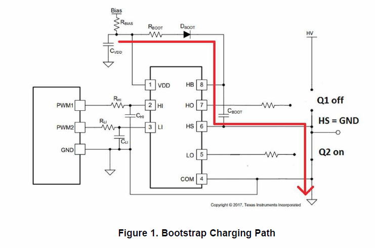
enter image description here

Then at some later point, the high-side switch will be commanded to conduct. When this happens, current will flow through the load and produce a voltage drop across the load which will cause the voltage at the MOSFET source pin (measured relative to ground).

Since the bootstrap capacitor negative terminal is also connected to this node the voltage at the cap negative terminal (measured relative to ground) will rise and consequently the voltage at the cap positive terminal (measured relative to ground) will also rise.

Normally this would raise the potential at the capacitor positive terminal above the gate drive supply and would discharge the cap to match the supply. But the bootstrap diode prevents this. In that way, the voltage across the capacitor terminals can be stacked on top of the high voltage supply when the high-side switch conducts to maintain a volage difference equal to the gate drive supply across the boostrap capacitor, and thus across the gate-source of the high-side MOSFET. enter image description here
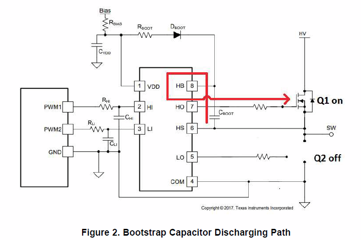
Taken from: http://www.ti.com/lit/pdf/slua887

This means two things for a bootstrap capacitor and diode high-side gate drive circuit:

  • a bootstrap high-side gate drive cannot achieve 100% duty cycle.
  • you need a low-side switch to recharge the capacitor (or some extra fancy charge pump circuitry)
\$\endgroup\$
7
  • \$\begingroup\$ So does this mean the Bootstrap capacitor needs to be rated for the HV supply? \$\endgroup\$ Commented Jun 22, 2022 at 2:39
  • \$\begingroup\$ @BigChungus443 No, because the high voltage never appears across it. It's the bootstrap diode that has to be rated for the high voltage supply. \$\endgroup\$
    – DKNguyen
    Commented Jun 22, 2022 at 3:02
  • \$\begingroup\$ Correct me if I am wrong, but once the MOSFET begins to turn on due to the capacitor, doesn't the High Voltage flow from the source of the MOSFET into HS and out of HO where it combines with the voltage that the capacitor is supplying to the gate? Or is that completely wrong :/ \$\endgroup\$ Commented Jun 22, 2022 at 3:32
  • \$\begingroup\$ Edit: if that is completely wrong, what is the purpose of the Vs pin? Is it really only there to discharge the top mosfet gate? \$\endgroup\$ Commented Jun 22, 2022 at 3:38
  • \$\begingroup\$ That's wrong because the path you just described is not a loop with the HV source. It's a loop around the capacitor but there is no loop through the HV source. \$\endgroup\$
    – DKNguyen
    Commented Jun 22, 2022 at 3:39

Your Answer

By clicking “Post Your Answer”, you agree to our terms of service and acknowledge you have read our privacy policy.

Not the answer you're looking for? Browse other questions tagged or ask your own question.