4
\$\begingroup\$

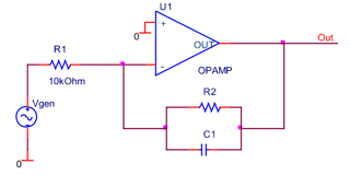
Our teacher explained to us that this set up allows us to produce the effect of a low pass filter:

enter image description here

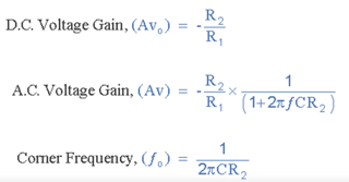
I have indeed found useful formulas to achieve this.

enter image description here

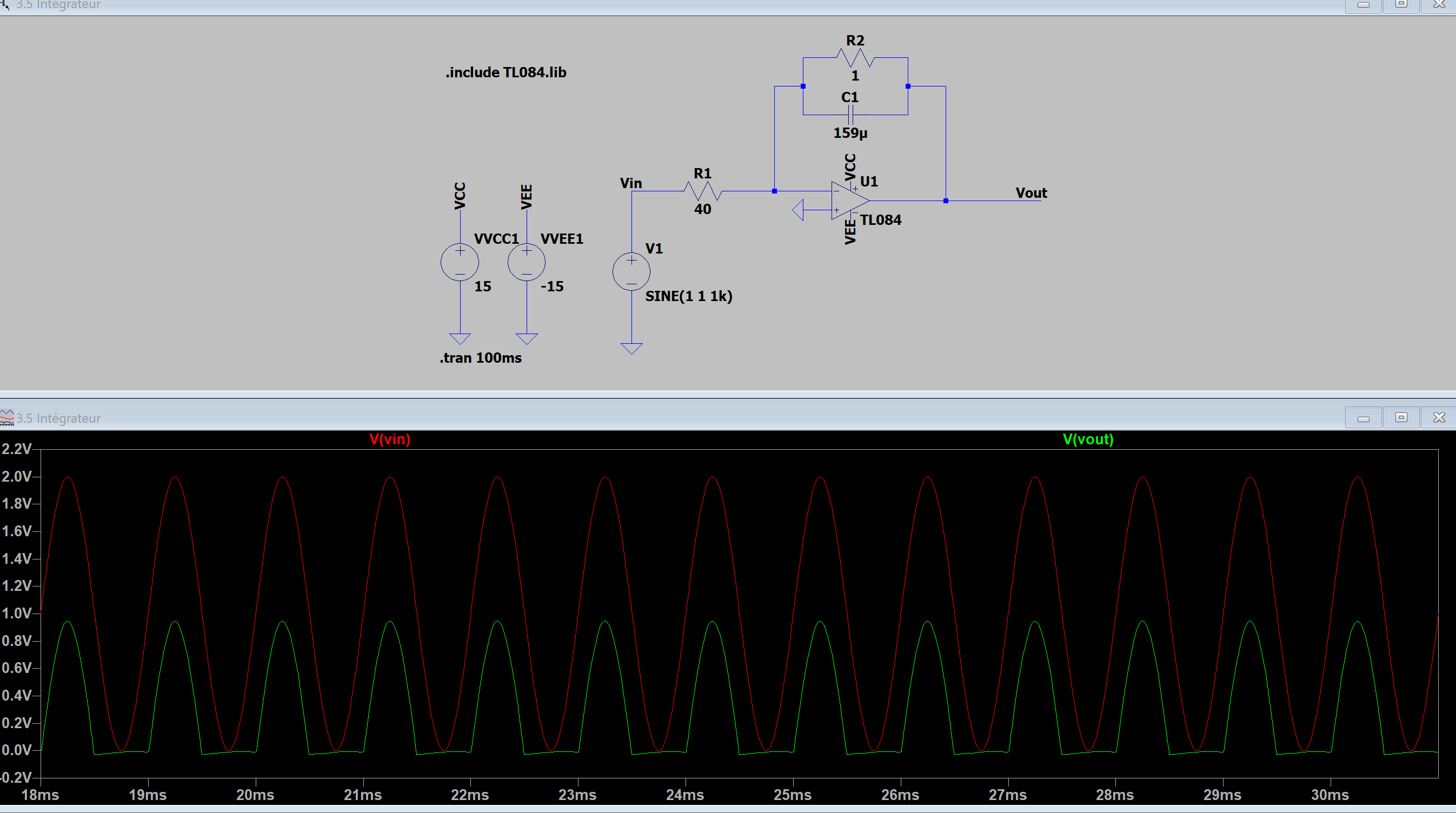
The problem however is that when I simulate this block on LTspice for a sinusoidal signal having a certain offset. The output voltage is not centered on this offset but on 0 V. Moreover the signal seems to saturate at 0 V whereas my op amp is powered between +15 and -15 V.

How to make sure to cut the frequency while remaining centered on the offset in order to tend towards the average of the basic sinusoidal signal?

enter image description here

For information, I have the same problem with a universal op amp and also if I use a square signal.

EDIT:
Here is what I get for R1=R2=10k and C1=15,9nF: enter image description here And for R1=100k R2=10k C1=15,9n: enter image description here
\$\endgroup\$
2
  • \$\begingroup\$ Your circuit has a gain of less than 1 which not all opamps are happy about but more importantly, your opamp does not have enough output current to cause any voltage drop to speak of across your 1 ohm resistor. Try increasing your resistances by a factor of 1-10k. \$\endgroup\$
    – winny
    Commented Mar 4, 2023 at 13:18
  • \$\begingroup\$ I tried R1=40k/R2=1k and R1=400k/R2=10k and it's still centered on 0V. Also I have the same problem if I replace this op amp with a UniversalOpAmp2 \$\endgroup\$
    – c.leblanc
    Commented Mar 4, 2023 at 13:50

2 Answers 2

5
\$\begingroup\$

The output voltage is not centered on this offset but on 0 V

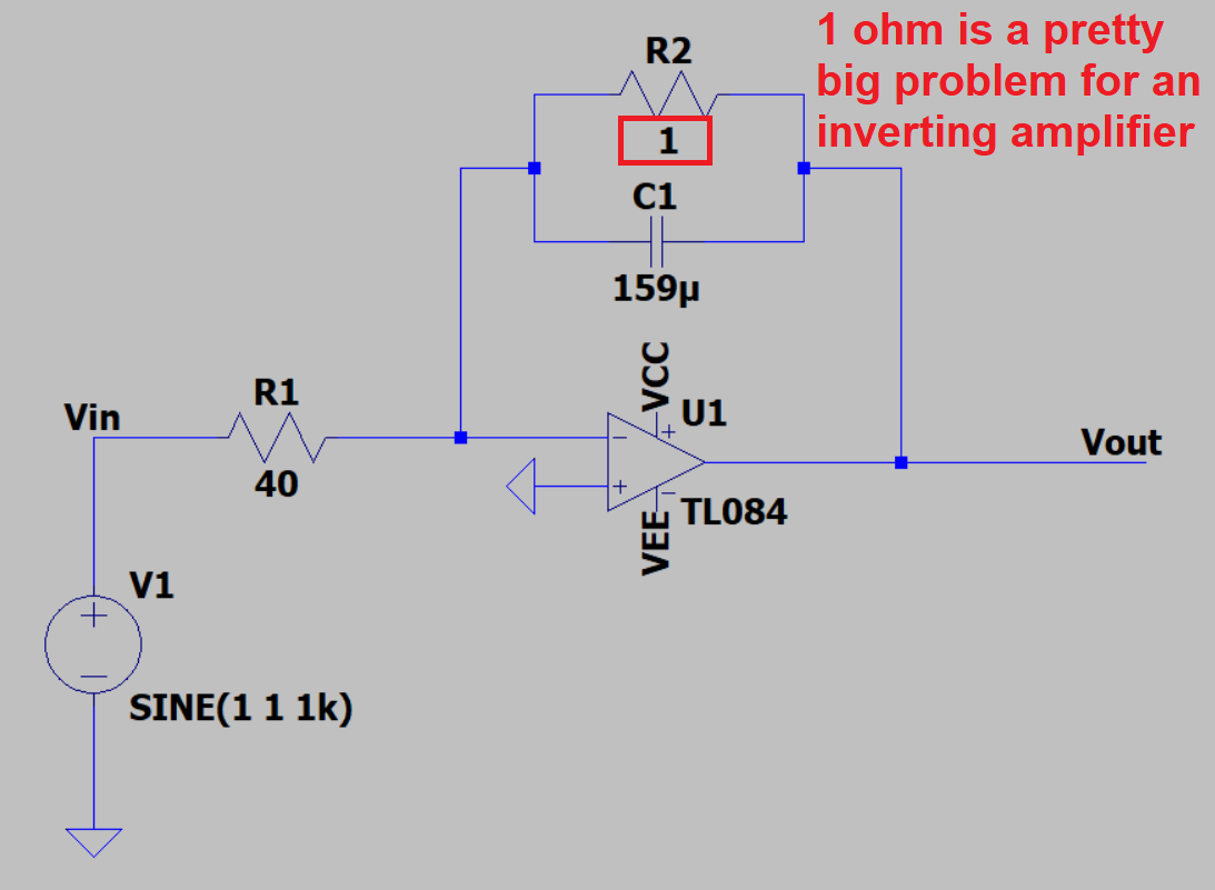
That's because of R2 is massively, massively too low in value. Take note of this: -

enter image description here

Try R1 = R2 = 10 kΩ. And, reduce C1 10,000 × in value to 15.9 nF.

Short story: use values that the op-amp can cope with.


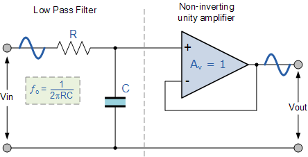
If you want a low-pass filter (it will maintain the same DC voltage level), you need a resistor and capacitor and, possible a unity gain op-amp buffer on the output to prevent load currents affecting the cut-off frequency of the RC filter: -

enter image description here

Image from here.

\$\endgroup\$
8
  • \$\begingroup\$ I posted the result of your suggestion in the edit of the main post. So, now I get the same signal as Vin (normal since R1=R2 ?) but in negative (I guess the bloc has a minus sign in the output tension?). But then if I want to reduce that signal by increasing R1, the amplitude of Vout decrease but also the center also moves (actually it moves so the maximum peak of Vout is always near 0v). Is there still a way to use this block as a proper lowpass ? \$\endgroup\$
    – c.leblanc
    Commented Mar 4, 2023 at 14:01
  • 1
    \$\begingroup\$ Yes, it's an inverting op-amp configuration and you get an average output level of -1 volts for a positive average level of 1 volts at the input. Maybe you need to explain what you are trying to achieve? If you want a low-pass filter that maintains the same DC voltage level, you don't need an op-amp; just a resistor and capacitor. @c.leblanc and, if you want to buffer the output so loading doesn't disrupt the amplitudes, use an op-amp unity gain buffer on the output. \$\endgroup\$
    – Andy aka
    Commented Mar 4, 2023 at 14:08
  • 2
    \$\begingroup\$ You are trying to use it in a way that doesn't match what you want to achieve (and I'm unsure what you are trying to achieve based on what you say). If lowering R2 reduces the output level magnitude it will also reduce the DC output level magnitude. Decide what you want to achieve and, if the inverting op-amp doesn't match those requirements then use what I said in my earlier comment. You won't make an inverting op-amp have an output DC voltage level that is the same as the input DC voltage level. \$\endgroup\$
    – Andy aka
    Commented Mar 4, 2023 at 14:21
  • 2
    \$\begingroup\$ Well, it's a basically a signal inverter so, if you want the same DC level on the output as that applied to the input, you need a different circuit. Analysing a circuit to understand what applications it is suitable for is probably not going to be very fruitful. I think I have answered your question. \$\endgroup\$
    – Andy aka
    Commented Mar 4, 2023 at 14:29
  • 2
    \$\begingroup\$ I can't help you with your future project but I can link you a data sheet for a typical op-amp (the LM324) that has several (26) applications towards the end: ti.com/lit/ds/snosc16d/snosc16d.pdf <-- a lot of them are for the inverting configuration @c.leblanc \$\endgroup\$
    – Andy aka
    Commented Mar 4, 2023 at 14:56
4
\$\begingroup\$

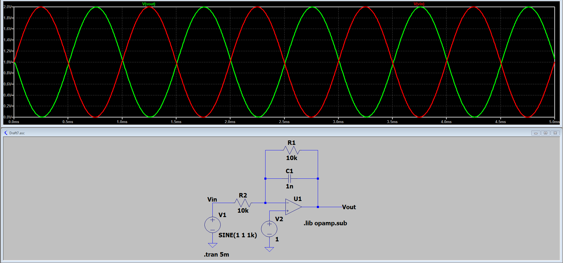
The inverting amplifier will invert your signal against whatever voltage is at the non-inverting terminal. If you notice, your plots using the larger resistors (after you fixed that problem) has an output signal flipped about 0V...and that makes sense since you've simply grounded your non-inverting input. However, if you apply the same DC voltage as your sine wave offset to the non-inverting input, your output signal will now be inverted against that offset:

enter image description here


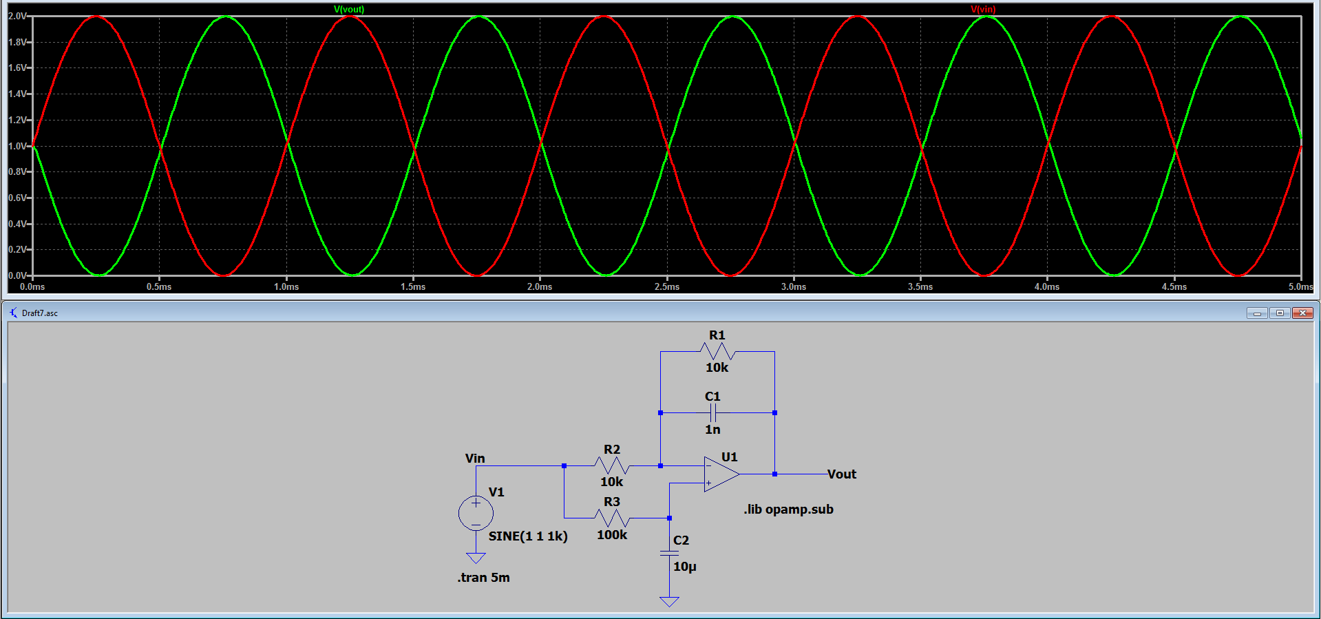
This is quite impractical, though, as you need to match the DC offset of whatever your input signal is. You'll either have to know that ahead of time and it has to be constant, or you need to extract the DC offset from that signal using a heavily low-pass filtered version of it and apply it to the non-inverting terminal. R3 and C2 does this below:

enter image description here


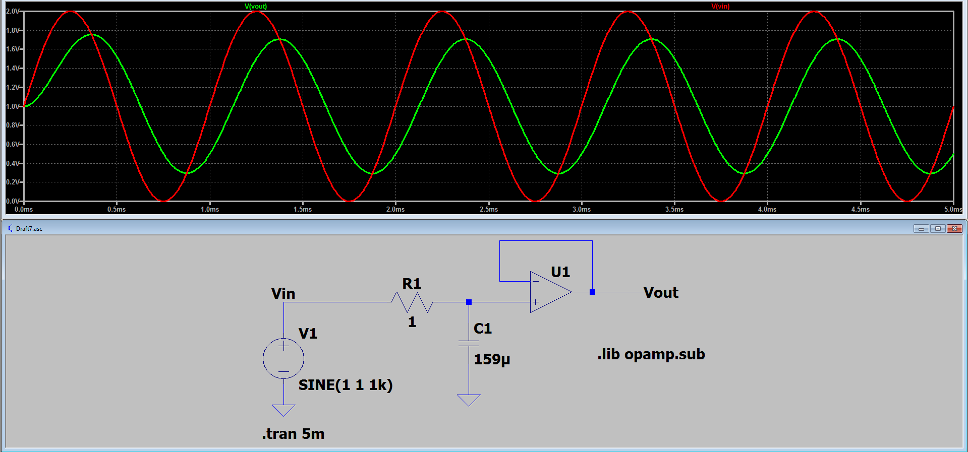
As Andy mentioned, at this point it's probably better to use either a passive low-pass RC filter and tack a non-inverting buffer after it if you need to isolate the loading effects, like so:

enter image description here

\$\endgroup\$

Your Answer

By clicking “Post Your Answer”, you agree to our terms of service and acknowledge you have read our privacy policy.

Not the answer you're looking for? Browse other questions tagged or ask your own question.