1
\$\begingroup\$

I've an exercise where I've to design an unbalanced differential amplifier, and I'm given the circuit below and told that it's the basic one. I'm then asked to have the appropriate bias resistors. enter image description here
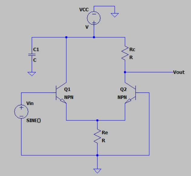
Are these resistors that I should add or do they correspond to Rc and Re? And how can I choose the appropriates values? (I'm free to choose all the characteristics of the circuit so I'm a bit lost)

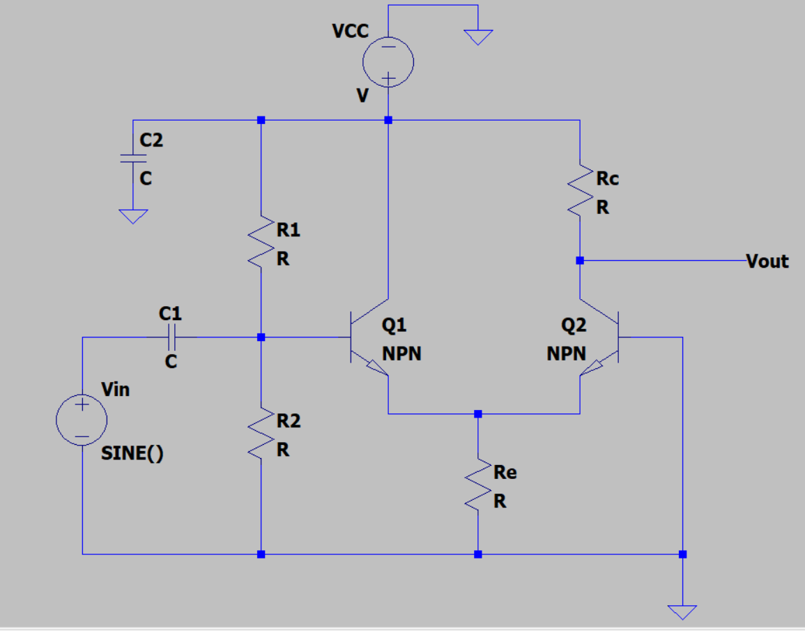
Edit: I added voltage divider resistors R1 and R2 for biasing, and a capacitor to isolate the DC value of Vin from its AC value. Is this new circuit correct? enter image description here
\$\endgroup\$
5
  • \$\begingroup\$ Differential amplifiers are normally (if not exclusively) designed to be "balanced". Why is yours unbalanced? What would be the point of this? Your output is single ended but, that doesn't necessarily mean it has to be unbalanced. A state of balance refers to impedances being balanced btw. \$\endgroup\$
    – Andy aka
    Commented Mar 20, 2023 at 22:39
  • \$\begingroup\$ Any other specifications? Or is the diagram all there is? (Unbalanced means that there will be more of an Early Effect problem than otherwise. But no big deal for education purposes.) \$\endgroup\$ Commented Mar 20, 2023 at 22:49
  • \$\begingroup\$ I don't know why they chose an unbalanced ampifier but it has to be like that. And I don't have any other specifications, it just has to be based on this basic circuit. \$\endgroup\$
    – Ekare
    Commented Mar 20, 2023 at 23:06
  • 1
    \$\begingroup\$ Are you sure that the base of Q2 ties to GND? \$\endgroup\$
    – tobalt
    Commented Mar 21, 2023 at 7:29
  • \$\begingroup\$ Yes, this is the principle of an unbalanced differential amplifier. \$\endgroup\$
    – Ekare
    Commented Mar 21, 2023 at 18:13

1 Answer 1

1
\$\begingroup\$

Not going to do your exercise, but I'll give you some tips. First off though, I find it hard to believe that you were given this assignment without a discussion of biasing BJT common emitter circuits. This circuit is very similar. Rc and Re are not the bias resistors. You need to alter the base connections and add some resistors so that some current can flow from the base to the emitter.For the circuit to work there needs to be some quiescent current flowing in each transistor, all of which ends up through RE, which elevates the emitters. As drawn Q2 would be reversed biased, if any current flowed in RE. Q1 may or may not depending on Vin's DC value. Of course there is no way for current to actually flow unless the transistors are biased correctly. Pick a voltage for Re that works, considering Rc. Then alter the base connections, and use some resistors in a way that make the base voltage correct for the emitter voltage that you have decided upon. Make sure that the resistor values chosen allow enough current to flow, and the resultant voltage isn't very sensitive to the amount of base current. There is a part that can isolate the DC value of Vin from its AC value. You may need that part.

\$\endgroup\$
1
  • \$\begingroup\$ This is the first really free design exercise, previously we were usually guided step by step with an already given circuit.Before starting my calculations, can you confirm that the new circuit is correct? I have tried to base my calculations on the circuits studied previously, taking into account your advice. \$\endgroup\$
    – Ekare
    Commented Mar 21, 2023 at 18:12

Your Answer

By clicking “Post Your Answer”, you agree to our terms of service and acknowledge you have read our privacy policy.

Not the answer you're looking for? Browse other questions tagged or ask your own question.