3
\$\begingroup\$

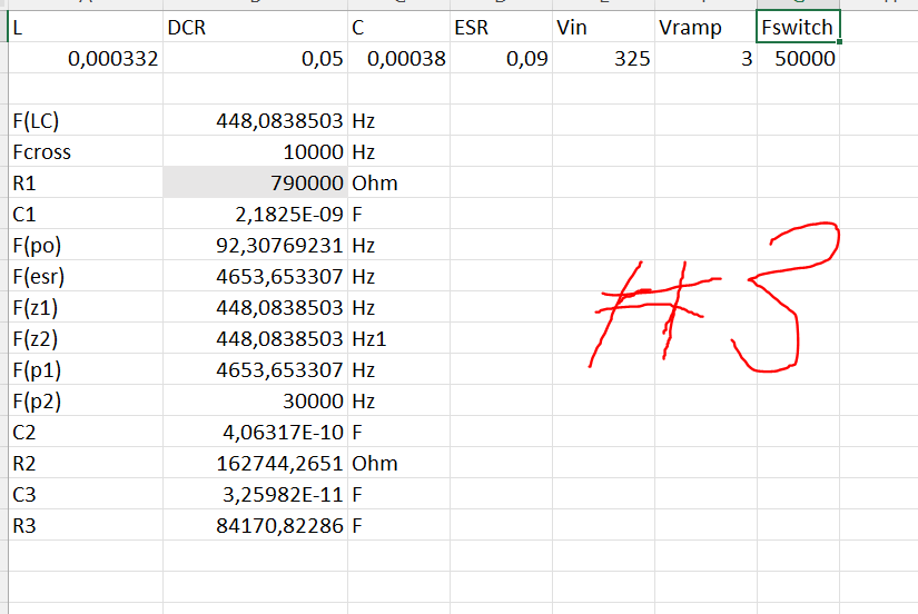
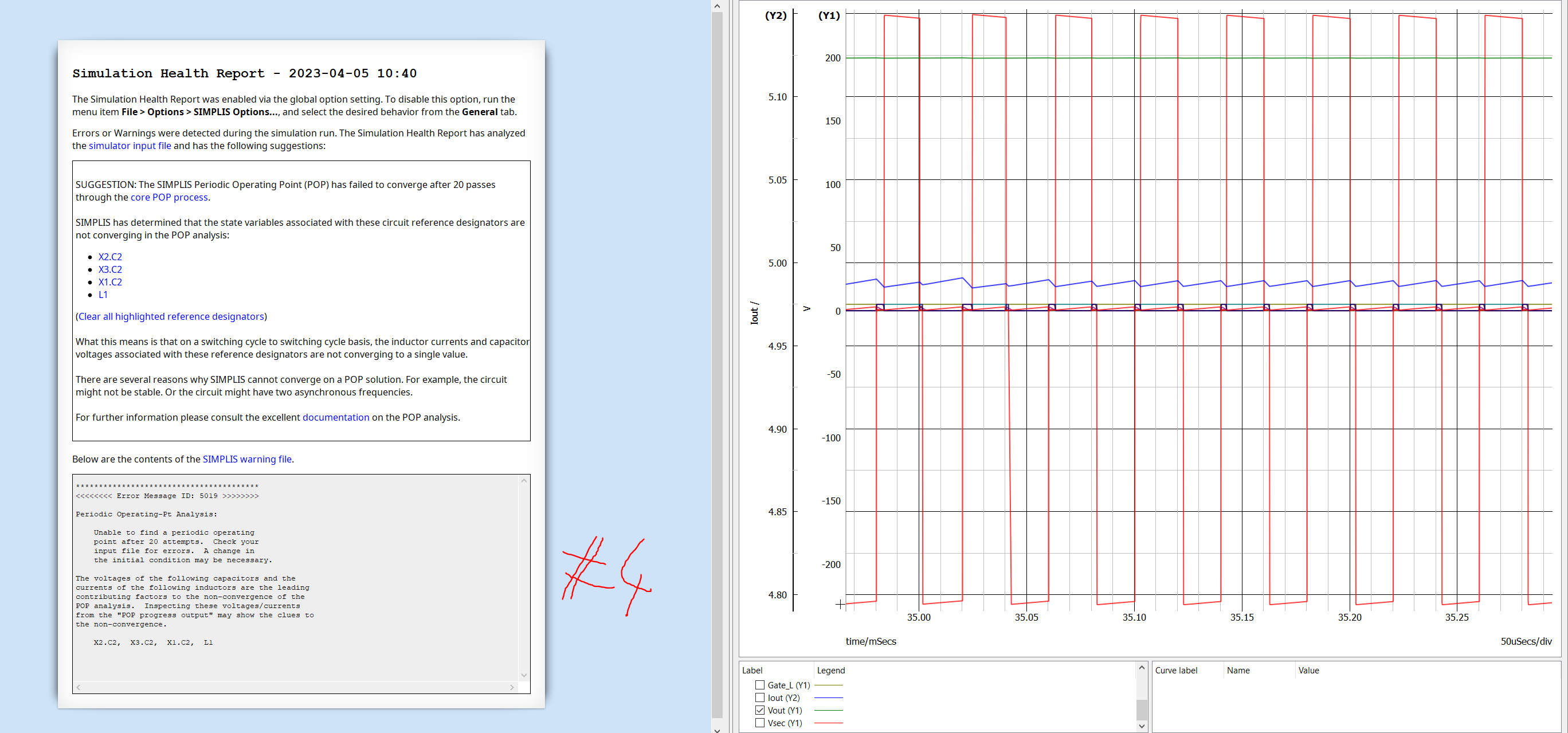
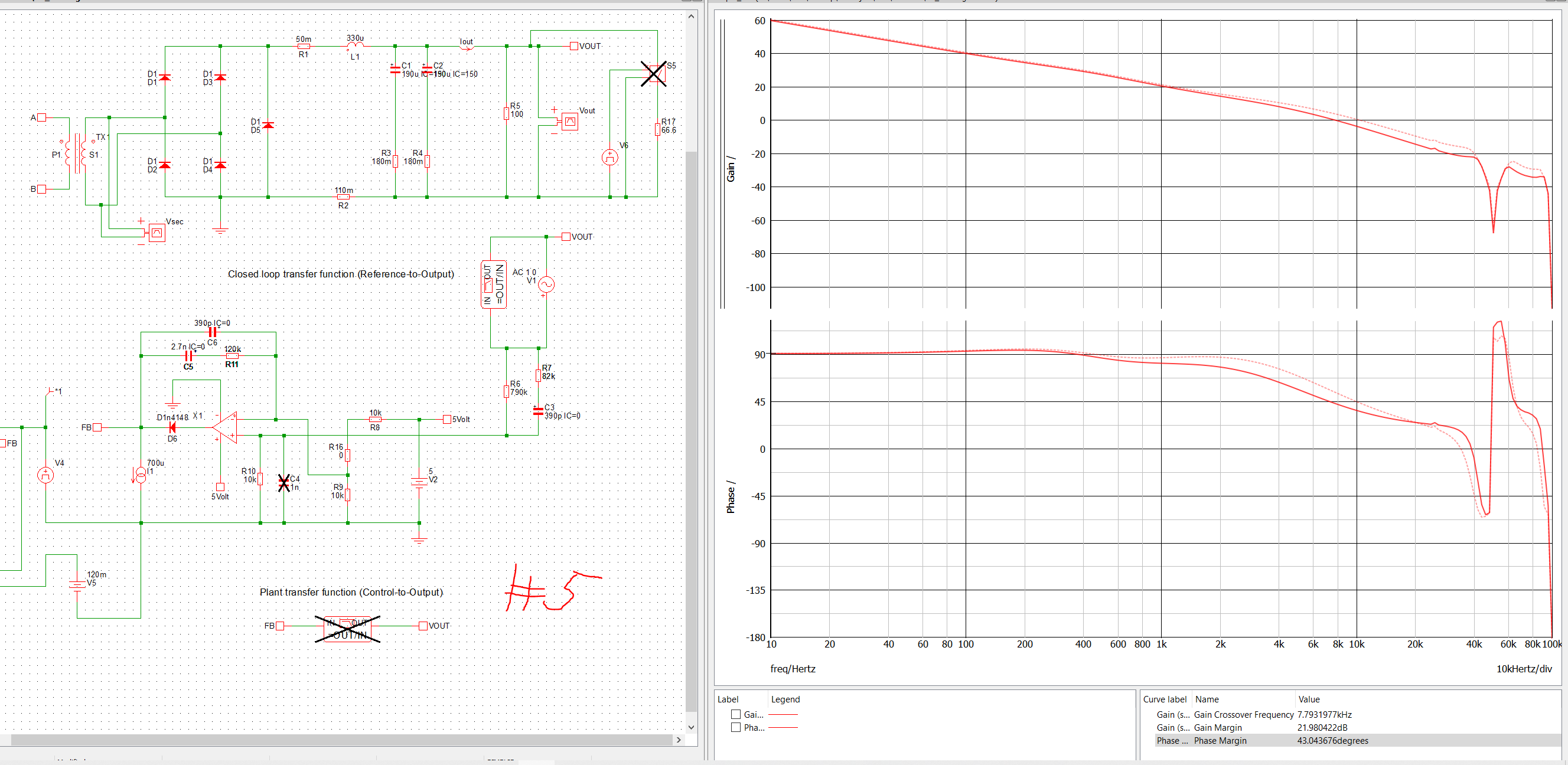
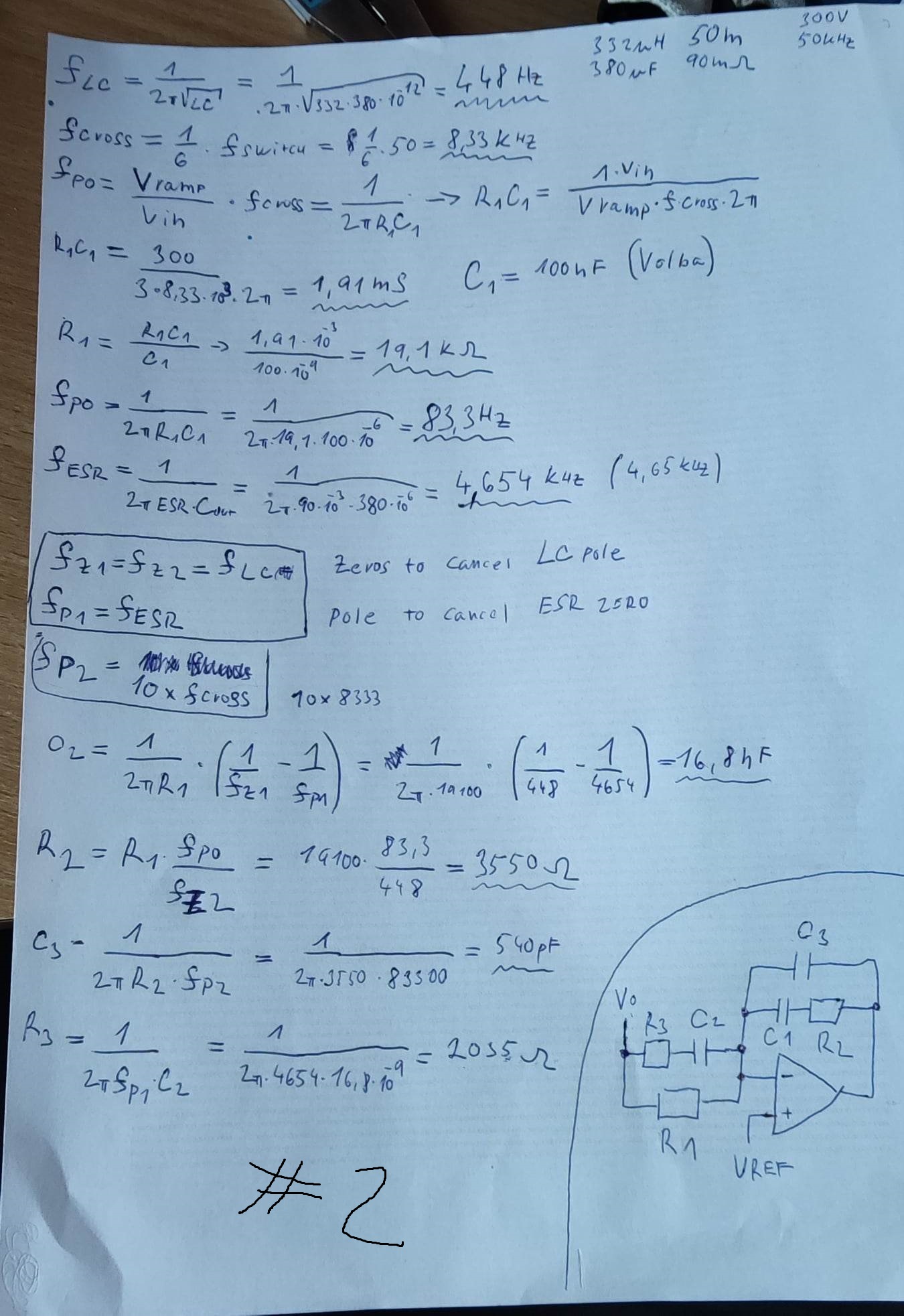
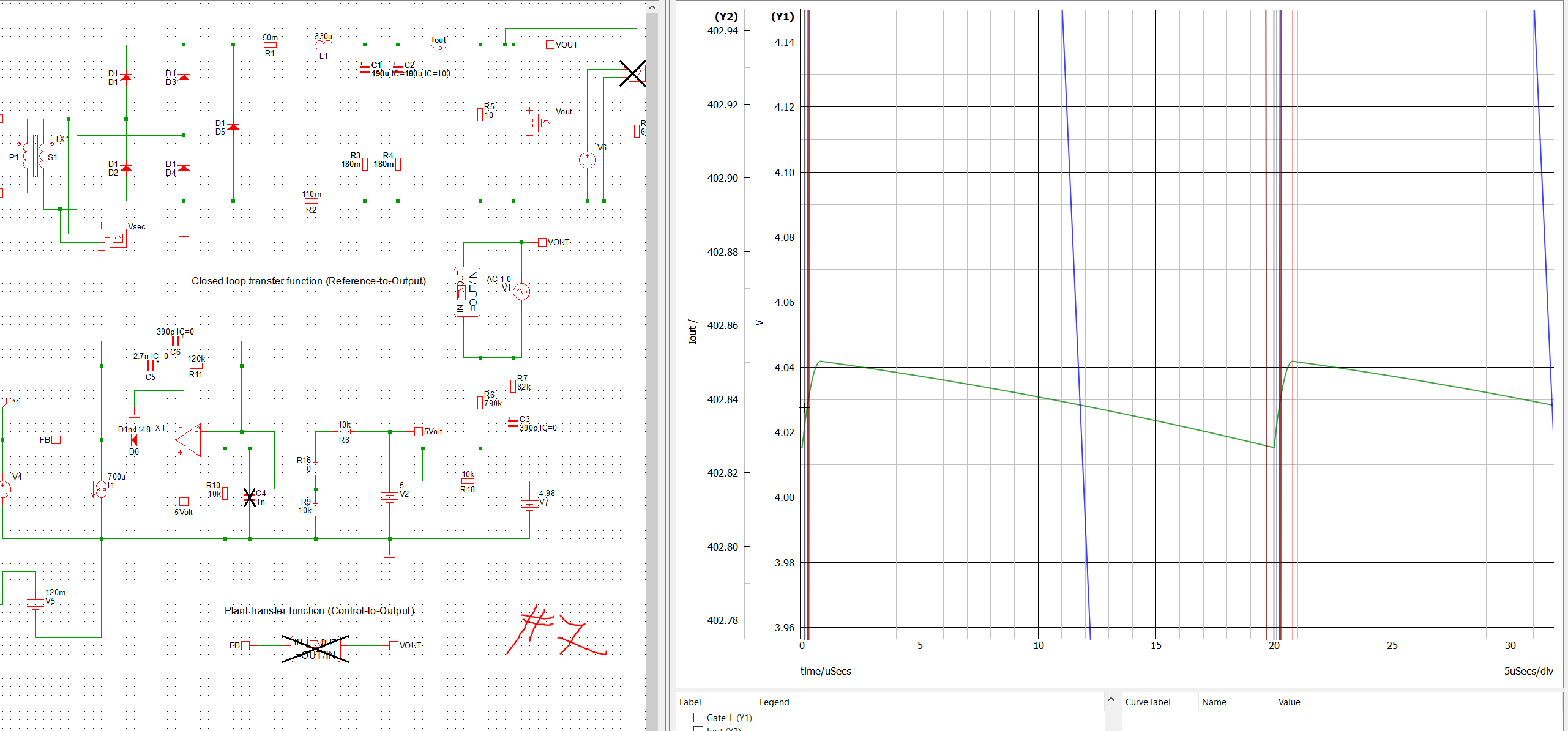
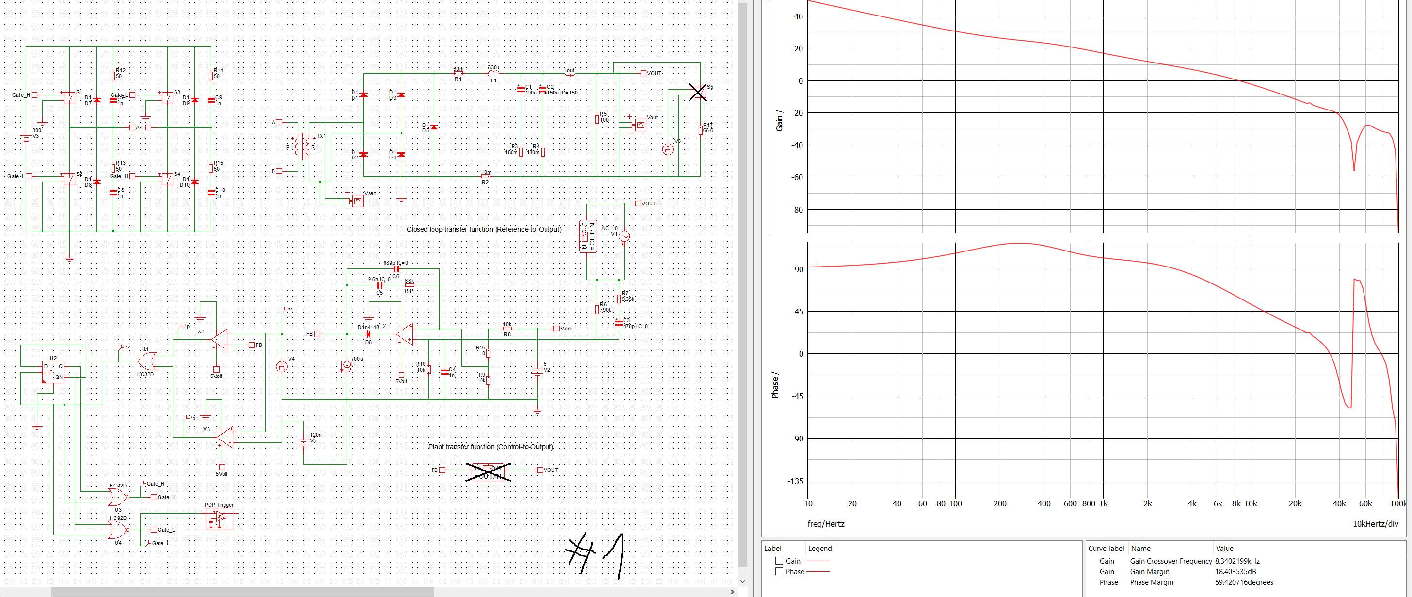
Hello i would like to ask how is compensation done on switching PSU with wide range variable output voltage (from zero to several hundres of volts). I have succesfuly (I guess) simulate my own design with simplis (picture #1). I am using TL494 which needs non-inverting type 3 compensation, i have played around values calculated thanks to @VerbalKint in this topic TL494 compensation. I have tried to calculate values at my own. I have follow steps in book "Switching Power Supplies A to Z from Sanjaya ManiktalaL" in chapter "Feedback Loop Analysis and Stability" page 481, second edition. Delivered values need some sort of tweaking, There was need to increase number of iterations in POP... ) Failed run at Picture #4. I actually dont know if this is the correct way to calculate it, i played with values anyway, result #5. So if @VerbalKint is reading this topic can you please tell in which book did you find the right procedure? Maniktalal procedure at #2, used values at #3.

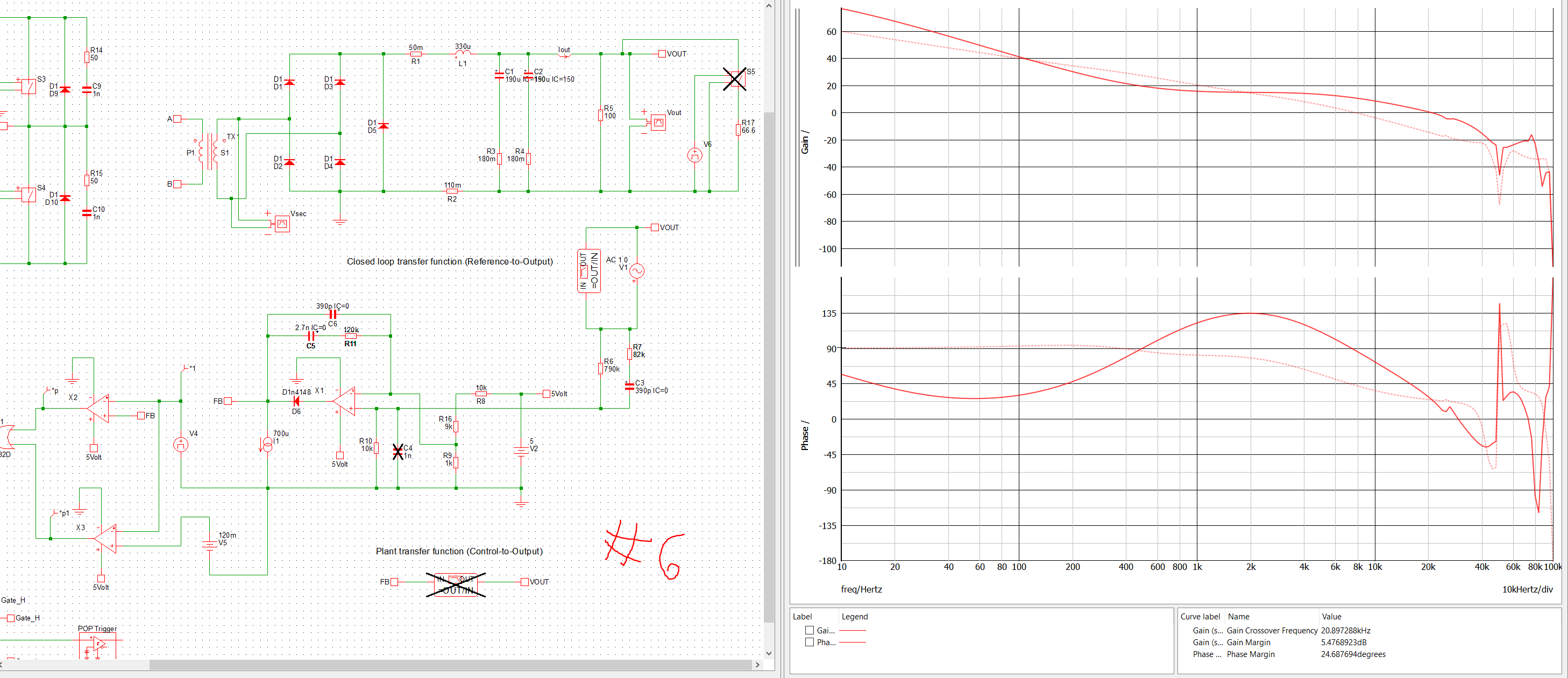
The main question is how its done at wide range output voltage. If you look at picture #6 (using setup from #5) i have changed reference voltage to have 20V at output (with resistor divider/ potentiometer) and as you can see phase and gain is completely different. How to face this? I have seen lab PSU from HSPY on ALI with range 0-1000V. How to stabilize this? Also they are probably using for reference voltage PWM output from MCU connected to RC network maybe with buffer at output? If someone know more details about that i would appreciate it. A Thanks very much

enter image description here

enter image description here

enter image description here

enter image description here

enter image description here

enter image description here

\$\endgroup\$
2
  • \$\begingroup\$ You cannot apply a conventional design procedure in your case because the TL494 requires a non-inverting op-amp which is totally uncommon. Guidance for placing poles and zeroes can be found in my blue book on loop control but all compensators are inverting. Equations for determining the poles and zeroes are given in the post I contributed, some more work is required to determine resistors values for an exact gain but nothing complicated I believe. Did you try? \$\endgroup\$ Commented Apr 8, 2023 at 15:45
  • \$\begingroup\$ @VerbalKint I did not, i didnt figure out how you came up with final values. After calculating Rlower there are values probably randomly picked just for starting point. I will take a closer look. Thanks for help =) \$\endgroup\$ Commented Apr 9, 2023 at 9:57

2 Answers 2

2
\$\begingroup\$

Keep the control loop constant.

You seem to be making the error that the impedance into -IN varies with setpoint, i.e. using a pot for R16-R9 (compare #5, #6).

Rather than connecting a potentiometer here -- and rather than trying to compensate with an inversely variable resistor in series to -IN -- simply buffer it: use another op-amp as voltage follower from the pot wiper, then connect a fixed resistor from its output to error amp -IN. (Evidently the series resistor should be 5k, since you compensated for a Thevenin resistance of R8 || R9 = 10k || 10k = 5k.) A much lower value pot can also be used (say 1k?) and a series resistor from the wiper (saves a buffer), or a 10k pot and a 47k series resistor, and then C5 and C6 go down by 5x and R11 up by 5x. (This is perhaps the less preferable option, since the high impedance makes the circuit more susceptible to noise.)

You can also connect a resistor from a variable voltage source to +IN, the summing node (a virtual ground -- not in the sense with respect to the error amp itself, but in the global sense, as the overall system has negative gain hence this is the negative feedback return point). This resistor does not participate in compensation (so no values need change), because this node is a virtual ground (ideally has zero voltage change), but simply tweaks the current flowing through R10 (i.e. acts in parallel with it), so adjusts the setpoint inversely with the applied voltage.

Note that a step change in voltage at -IN feeds forward into the modulator, creating a step change in PWM. This should probably be filtered off ahead of time (an inline RC filter?), so that a correct proportional response can be achieved. (The +IN input does not suffer from this mechanism.)

\$\endgroup\$
2
\$\begingroup\$

This website cover this topic https://eepower.com/technical-articles/dynamic-output-voltage-adjustment/#. I wish i have discovered it earlier =)

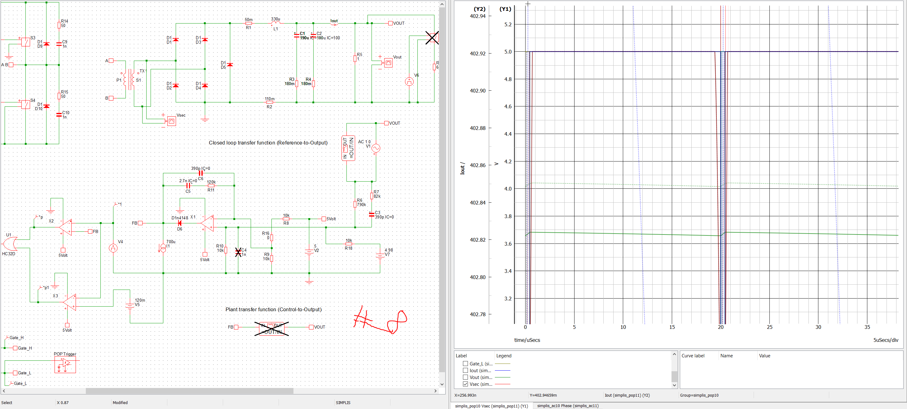
Now i need to solve how to solve feedback to have stable output voltage undependent on load. Pictures #7 and #8 show how load affect output voltage. Green line is Voutenter image description here

enter image description here

\$\endgroup\$
6
  • 1
    \$\begingroup\$ Could you edit your answer to include the details from the link? Otherwise this is a link-only answer. \$\endgroup\$ Commented Apr 6, 2023 at 13:39
  • 1
    \$\begingroup\$ MacIntoshCZ - Hi, As commented above & explained here, an "answer" which is just a link to another site (no matter how good or useful) is not an answer on Stack Exchange. || Also, since you asked the question, and have now provided (what you want to be) an answer, then the topic should now be considered closed & you don't want more replies, right? If that's not right, then this isn't an (attempted) answer. I'm unclear what state you want your question to have - please can you clarify? If this is the final solution, please can you expand it? Thanks \$\endgroup\$
    – SamGibson
    Commented Apr 6, 2023 at 14:37
  • \$\begingroup\$ Hi, i would not consider this as an answet yet. I have done some testing and it seems output voltage is not "HARD" enough, it depends on load. Its not big difference on higher voltages but when output is set to few volts, you can see a difference. I was injecting current with another voltage source through 10k resistor to R10. \$\endgroup\$ Commented Apr 7, 2023 at 6:14
  • 1
    \$\begingroup\$ To compensate at different operating points, you need to extract the control-to-output transfer function at all these different points and make sure the adopted compensation strategy in all cases leads to a stable configuration. This is key for the design of a stable converter operated across a broad range. \$\endgroup\$ Commented Apr 8, 2023 at 15:49
  • 1
    \$\begingroup\$ Hello @MacIntoshCZ, I have released a document showing how to place the poles and zeroes with a non-inverting configuration as with the TL494. The doc is available from my webpage here. It is not an obvious procedure considering the goofy architecture but it seems to work. Not sure how it behaves in large signal though. Good luck with this design. \$\endgroup\$ Commented Apr 11, 2023 at 6:21

Your Answer

By clicking “Post Your Answer”, you agree to our terms of service and acknowledge you have read our privacy policy.

Not the answer you're looking for? Browse other questions tagged or ask your own question.