1
\$\begingroup\$

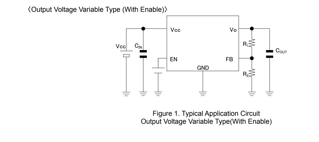
I'm trying to configure the regulator to output 4.5V. From what I gather, the output voltage is governed by the voltage divider between Vo and GND where the device's FB pin reads the voltage dropped across R2. However, as the applied voltage to the regulator changes, so does the output voltage. This seems like it will be a problem since the applied voltage will come from an unregulated battery supply of 4 NiMH batteries, which should drop from ~5.6V to ~4.8V before cut-off. If Vo changes depending on the applied voltage, how can a voltage divider be configured to maintain a consistent 4.5V for Vo?

Image from Datasheet here

enter image description here

The datasheet can be found at the following link: https://www.digikey.ca/en/products/detail/rohm-semiconductor/BD00FC0WFP-E2/7896451

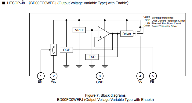
Below is a screen capture of the LDO regulator circuit diagram:

enter image description here

\$\endgroup\$
2
  • \$\begingroup\$ It would help if you include an image from the datasheet which shows the basic circuit configuration. \$\endgroup\$ Commented Jun 10, 2023 at 23:17
  • \$\begingroup\$ Data sheet is at link I've added. It's a standard Vout = Vref x (R2+R1)/R1 arrangement. | See page 8 - Vref = 0.75V. Output does NOT vary with Vin. \$\endgroup\$
    – Russell McMahon
    Commented Jun 11, 2023 at 12:24

1 Answer 1

0
\$\begingroup\$

It is understandable that you are confused since you can't see the inner workings of the regulator.
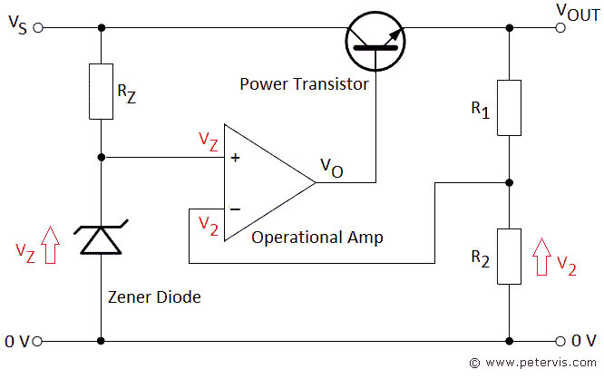
Here is an example schematic to help you understand what is going on (image/schematic taken from https://www.petervis.com/electronics%20guides/voltage-regulator-using-op-amp-and-transistor/voltage-regulator-using-op-amp-and-transistor.html): enter image description here

The way this circuit works is following:

  • Zener diode is a reference voltage which doesn't change, regardless of the input voltage, as long as the input voltage is above the zener voltage.
  • Let's say the zener diode in this case is 5.0V.
  • The way operational-amplifier (op-amp) works is that it tries to maintain the voltages on its inputs (+) and (-) equal to each other and its output goes positive if its (+) input goes more positive compared to (-) input, and more negative if (+) input goes more negative than (-) input.
  • If R1 and R2 are of equal values, the voltage between them will be half the output voltage. This also means that the Vout will be twice the voltage between the two resistors since they are dividing it in half.
  • Since zener voltage (Vz) and thus (+) input of the op-amp is at 5.0V, the op-amp will give out a positive voltage if the V2 is below 5.0V (Vout below 10.0V), which will drive the transistor to pass more current and raise the output voltage.
  • If the V2 voltage goes above Vz (above 5.0V, which happens when Vout starts going above 10.0V), the op-amp will start reducing its output current and going more negative, which will make the power transistor pass less current and start reducing the output voltage Vout.
  • The ratio of the R1 and R2 resistors determines the output voltage as compared to the reference or zener voltage: if R2 is 1/3 the value of the total resistance of R1+R2, the output voltage will be 3 times higher than the reference/zener voltage.
    However many times the two resistors divide the output voltage Vout, that many times will the output voltage be larger than the reference voltage Vz.

The formula for determining the output voltage is simple:
Vout = Vz x ((R1+R2)/R2)
or
Vout = Vz x ((R1/R2) + 1)

\$\endgroup\$
4
  • 1
    \$\begingroup\$ Would that mean, then, that the Rz and the zener diode shown in the circuit you posted are represented by the VREF block in the block diagram I added above? \$\endgroup\$
    – debounce
    Commented Jun 11, 2023 at 1:35
  • \$\begingroup\$ @debounce Yes, that's right. \$\endgroup\$ Commented Jun 11, 2023 at 5:30
  • 1
    \$\begingroup\$ Thank you for the explanation. Now that I had a better idea of what was going on, I consulted the datasheet again and found the output voltage reference value to be 0.75V using the formulas you provided (I also confirmed the value using one of the provided examples in the datasheet). Regulator is now working perfectly! \$\endgroup\$
    – debounce
    Commented Jun 11, 2023 at 6:30
  • \$\begingroup\$ @debounce You're welcome. As you may have guessed, the input polarities of your regulator's internal op-amp/comparator are reversed compared to my example, but that's because the output transistor works with opposite polarity drive - it is a P-channel MOSFET which requires a negative voltage to turn on (relative to its source pin which is on the positive input rail). If my answer is acceptable, you should mark it as "accepted answer". You may also upvote it at the same time, I think. And you did a good job on your part figuring out the Vref and getting it to work for you. You got my upvotes. \$\endgroup\$ Commented Jun 11, 2023 at 6:42

Your Answer

By clicking “Post Your Answer”, you agree to our terms of service and acknowledge you have read our privacy policy.

Not the answer you're looking for? Browse other questions tagged or ask your own question.