Wanting to remove common mode noise (CMN) from my USB data line (12/1.5 Mbps speeds) I use common mode choke.
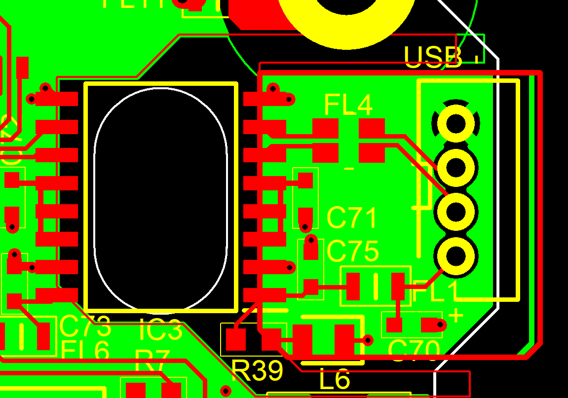
My layout is shown below. FL4 is the common mode choke (DLW21HN181SQ2L), and IC3 is a USB isolator ADUM3160. The GND plane is split and my design works as I expect it to be.

I want to take it a step further, and I wonder if removing the GND plane under the USB traces makes sense, (similar idea/question here) since the GND plane will carry CMN, and I suppose CMN will affect the USB data lines after the common mode chock. So at the end I think the common mode chock will have no effect at all (or very little effect) if I have the GND plane underneath it.
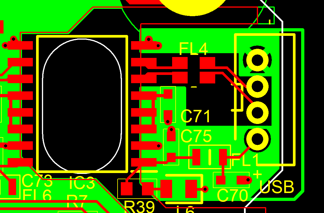
So I am thinking removing the GND plane like that:

Since USB (data lines) need GND only for the handshake, removing the GND plane under the data lines wont affect the signal integrity (hopefully) and I suppose it will do a better job in keeping CMN away from my data lines.
(Side note: My design is in metal enclosure with AC input, so metal enclosure is tied to earth)
- Has anyone tested such layout?
- What I say makes sense?
- What problems could that layout cause?
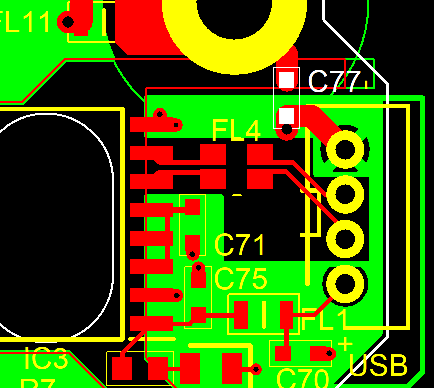
As an extra update to the board, I will try adding a capacitor (C77) between the GND and earth in case it also helps removing CMN. (Idea from here)

