I'm trying to upgrade the storage in a consumer device by swapping in a larger NAND chip (specifically a Micron MT29F128G08CFABBWP). After modifying the firmware to accept the chip's ID and geometry, the first thing it does is attempt to format the chip with some metadata on the first several pages of the device. However, when it hits the 7th page (address 0x0000060000), and every page thereafter where the page address has a high bit 1, I observe that the program time takes longer than the "good" pages and, when the data is read back to verify it, it's exceptionally noisy.
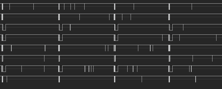
For the "good" pages, tPROG is right around ~600μs and the verification reads are pristine. For the "bad" pages, tPROG is ~1700μs (still in spec, but weird), and when the device reads the data back, it's wrong in a way I can only describe as "noisy". I'm examining this behavior with a logic analyzer, and it's quite obvious from the capture that it's noisy because most of the data written is 0xFF and the capture that comes back is not the same.
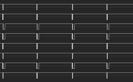
Here's a snippet of the I/O lines during a clean readback:
And here's the ugly verification read of page 7:
(images not to scale)
This is true across all blocks of the device.
I would understand if this phenomenon occured on one chip in isolation. But this is the third chip I've tried and have observed the same results. I do not understand what could be going on.
Some things I've considered:
- I figure it could be bit errors, and I would understand a handful of them happening randomly across any pages being accessed. But the pattern of which pages are good and which ones are bad is very predictable. And this feels like a lot of bit errors.
- This chip works within the same voltage range as the original chip, but probing the chip's Vcc with an oscilloscope shows that it may be browning out for a few nanoseconds, but it seems to do this even for successful read/writes. After adding a decoupling capacitor to the line, I've been able to keep it from dipping below its minimum recommended voltage (2.7V). I've also modified the code to raise Vcc from the default 3.0V to 3.3V and even 3.4V so it stays even further away from the lower bound. Still, the problem persists.
- This NAND chip might have a quirk I'm unaware of, but the datasheet doesn't make a mention of dragons with page address bit #1. I don't think I'm accidentally targeting another LUN.
- The logic analyzer and its associated setup extends the traces beyond reasonable distances and has occasionally caused the interactions with the chip to fail. To counter this, I have modified the firmware to go as slow as possible (I believe it's operating with Mode 0 timings now based on the speed of RE/WE). This ensures consistent results every time I run it.
- The new chip uses a different NAND technology (SLC before, MLC now). But, with my limited understanding of the differences, I don't see how that could cause this.
I've truly run out of ideas here. I don't know enough about NAND to know why this is a problem in this specific scenario. What could possibly be causing this?
Thanks in advance for your help. If I left out any key information or if there's something I've forgotten to try, let me know. I'd really like to get to the bottom of this!
Edited: I've discovered that, while the issue begins on Page 7, there exists a pattern of good pages and bad pages. This makes it less baffling but brings me no closer to the answer.


