0
\$\begingroup\$

enter image description here

My Power System, can someone validate it? I'm not familiar with using the TPS63060.

Datasheet can be found at: https://www.ti.com/product/TPS63060

I'm trying to power a ATMega328p-AU + 4 digit 7-segment display. I'm not trying to do something overcomplicated, just run the circuit for a reasonable amount of time, at a good efficiency which is why I opted out of using a Linear Voltage Regulator.

It is to run a clock, a very simple gift I'm trying to design. My goal is to create a 3V3 output from the below circuit. The TPS63060 is a high input voltage buck-boost.

Input: The power source is 4 x AAA cells in series at 1.5 V each, totaling at 6 V.

PS: I'm a absolute beginner at electronics so any recommendations/ knowledge would help a lot. Thank you to everyone who takes the time to help me and point me in the right direction.

Edit and New: Thank you to everyone for the candid feedback, I needed it. I apologise for the rampant errors, I have no answer for it, here's the new schematic I'd love to know your thoughts on, please let me know if any mistakes persist.

enter image description here New Schematic

\$\endgroup\$
6
  • 1
    \$\begingroup\$ 1. Place output capacitors on Vout pin. 2. Check, if feedback resistance can be increased, if you want to reduce static power consumption. 3. Check if part disconnects load, if enable tied low, if you wnt to control converter with MOSFET instead of switch. \$\endgroup\$ Commented Feb 29 at 13:08
  • 1
    \$\begingroup\$ The caps on VIN, VOUT and FB are missing. The caps between PAD and GND make no sense. \$\endgroup\$
    – Velvet
    Commented Feb 29 at 13:10
  • 1
    \$\begingroup\$ You're trying to build fig. 9 in the datasheet with a slightly different voltage, so you can use that as is except with a different feedback resistance. If you hook up something different than fig. 9 (like most of your capacitors), good chance it's a mistake. \$\endgroup\$ Commented Feb 29 at 13:25
  • 1
    \$\begingroup\$ There is no description of what the circuit must do and what components are used. So even if the schematics were correct and component values correct too, you still might have picked incorrect components. Please list all components and link to their data sheets. \$\endgroup\$
    – Justme
    Commented Feb 29 at 13:56
  • 1
    \$\begingroup\$ I would suggest getting a SMPS module where the whole circuit is already designed and integrated into a single package - designing a SMPS is complicated when you have little experience; it's not a beginner project. I'm calibrating your experience based on the fundamental mistakes observed in your schematic. Consider a 3.3V buck POL convertor. They are simple to use 3-terminal devices with excellent efficiency. \$\endgroup\$
    – MOSFET
    Commented Feb 29 at 15:13

3 Answers 3

4
\$\begingroup\$

There are a lot of changes to make. One must be very careful to check and re-check the process of transferring schematics to layout. I double-check the transfer from schematic to layout, then put it aside for another day - then double-check again. That second-day check has found enough errors to boost its importance in my mind.
In this case, I've only single-day checked your schematic, so I may still have missed an error. It is disturbing to me that so many errors were found. You should be much more careful.
Your schematic is re-drawn below (electrical engineers regard schematics as a kind of gold-standard document) including many corrections. Below that, a change-list has been added, so you don't miss one...
updated schematic diagram

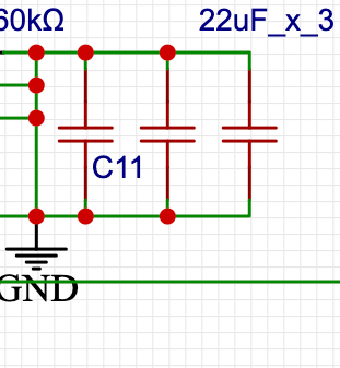
  • disconnect C11 group-of three from FB pin 8. This group-of-three has its top-end going to GND - this is wrong.
  • ensure that FB pin 8 is not connected to GND - FB pin 8 should only go to three components: R13, R16, new ?pf capacitor.
  • connect C11 group-of-three to Vout pin 9. Other side of C11 is GND.
  • change R13 from 100k to 560k
  • change R16 from 560k to 100k
  • disconnect PG pin 5 from VCC
  • add new pull-up resistor (100k suggested) from PG pin 5 to VCC. This can be used as "power-good"...a good way to save processor state if you lose power.
  • add 2x10uf capacitors from Vin pin 2 to GND
  • add ?pf capacitor from FB pin 8 to GND.
  • ensure that PS/SYNC pin 4 routes to GND.
  • ensure that each GND on that schematic links to every other GND. These GND links should be short and robust - meaning that they should be broad-width having low inductance. The GND path to your processor should be similarly robust.
  • It is perhaps unclear from my re-drawn schematic that C10 (100nf) does NOT connect to the new ?pf - C10 connects from VAUX pin 6 directly to GND. new ?pf connects only from FB pin 8 to GND pin 7.

I have used the data-sheet fig.8 as a guide for these changes. The new capacitor ?pf is important for stability. Its value should be carefully determined from the design guide in the data sheet.

\$\endgroup\$
4
  • \$\begingroup\$ Thanks my man, I'm very sorry the plentiful errors. Your response was clean and direct, I appreciate that. I've updated the question with the new schematic with feedback taken from your answer. Please let me know your thoughts, also let me know if I should start a new question, or is this okay? \$\endgroup\$ Commented Feb 29 at 21:46
  • \$\begingroup\$ Your revised schematic edit is fine, and looks OK. When transferring to printed circuit, cross-check your layout with data sheet's 11.2 Layout Example, which has copper on at least two layers. Zener diode D1 is unspecified - it will have to pass all the battery input current: a low-current zener may over-heat. I hope you have a good outcome and gain confidence doing this project. \$\endgroup\$
    – glen_geek
    Commented Mar 1 at 17:57
  • \$\begingroup\$ Thanks Glen, I'll look into using a MOSFET to replace the diode. Let me know if you have a part I can use or any resources that can help with the same. I'll read 11.2 on the datasheet, and might post again with the PCB on the platform. Thanks for all your help and time, I appreciate it. By the way, from 11.2 how can you tell how many layers of copper exist on the PCB? Which are the obvious layers you can see? \$\endgroup\$ Commented Mar 1 at 20:34
  • \$\begingroup\$ Fig 11.2 shows four ground areas, each with vias - these must connect to a ground plane underneath (not shown). One of those four gnds has only one via, and is not labelled gnd. It does not carry heavy gnd current, but still must join to the other three grounds. Fig.11.2 shows only the layer where TPS63060 is soldered along with resistors, capacitors, inductor. \$\endgroup\$
    – glen_geek
    Commented Mar 1 at 23:22
1
\$\begingroup\$

You have shorted capacitors:

enter image description here

I think these are supposed to be placed across the output i.e. VCC and GND.


Place capacitor(s) across the input terminals, namely VIN and GND terminals.

enter image description here

The capacitors across the input may also help to tame the bouncing coming that possibly from the slide switch.


The typical application circuit given in the datasheet has a 10 pF across the low-side feedback resistor. You may want to place one across R16 in your circuit.


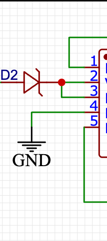
Finally, if D2 is there for reverse polarity protection then consider a MOSFET instead, because there's going to be a drop across the diode so the IC will see lower voltage and finally will draw higher currents. If you worry about battery life then this will become more important.


From the schematic, R13 seems to be 100k and R16 is 560k. This will not give you 3.3 V output. They should swap:

$$ V_O=\Big(1+\frac{R_{13}}{R_{16}}\Big) \ V_{FB}=\Big(1+\frac{560}{100}\Big) \ 0.5 = 3.3 \text{ VDC} $$

\$\endgroup\$
1
  • \$\begingroup\$ Thanks, Rohat. I'll consider adding a MOSFET next, I've fixed the problems you've mentioned and updates the question. Let me know if there's anything I can do more. Thank you for your time and effort. \$\endgroup\$ Commented Feb 29 at 21:47
0
\$\begingroup\$

The parts are unknown so we don't know if they will work.

However, you have drawn D2 as a Zener which makes no sense.

There are no input capacitors either.

PG is shorted to output so there will be damage to the IC.

Output has no caps and they are shorted instead.

FB capacitor is not present.

\$\endgroup\$
2
  • \$\begingroup\$ Thank you for taking the time, I've updated the schematic with feedback from the community. The new schematic is in the question, thank you for taking the time, I really appreciate all the help. \$\endgroup\$ Commented Feb 29 at 21:49
  • \$\begingroup\$ @MustansirGodhrawala The parts you used are unknown so you might have used parts that don't work. \$\endgroup\$
    – Justme
    Commented Mar 1 at 4:07

Your Answer

By clicking “Post Your Answer”, you agree to our terms of service and acknowledge you have read our privacy policy.

Not the answer you're looking for? Browse other questions tagged or ask your own question.