0
\$\begingroup\$

I'm building a boost converter from scratch and am planning to use an STM32 microcontroller to generate a PWM signal to regulate the output voltage. The power supply voltage of the circuit is 24 V, and I aim to adjust the output voltage from 24 V up to 100 V with a current of 100mA. Additionally, I want to read the output voltage value using the STM32 ADC input to adjust the PWM accordingly.

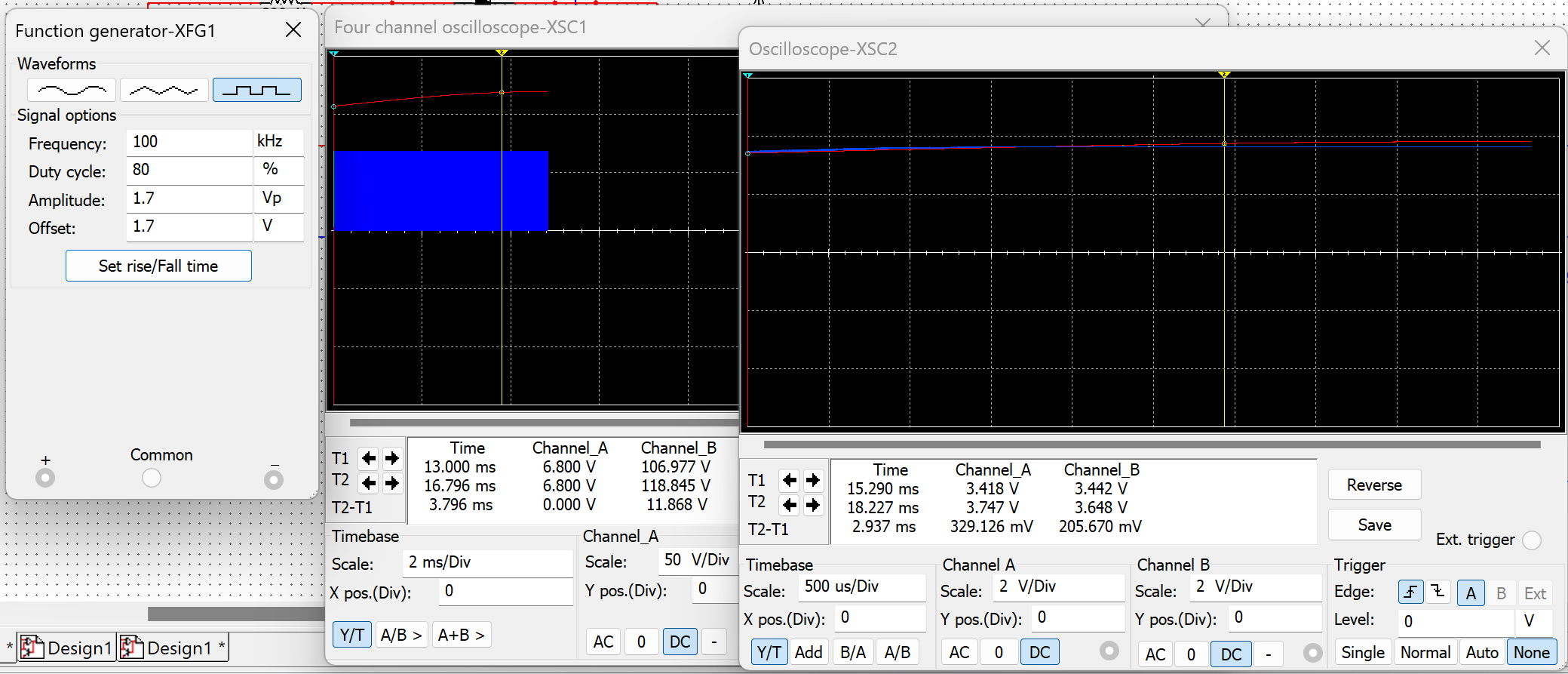
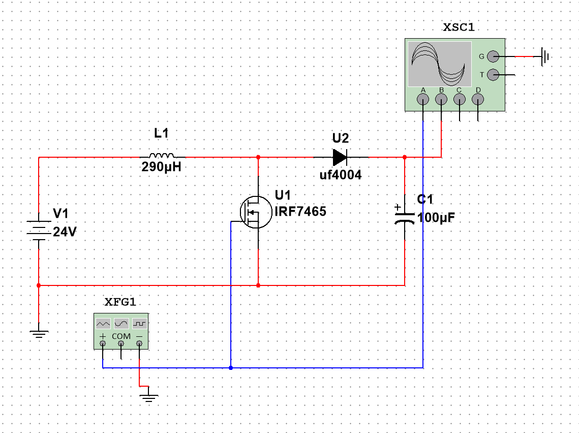
Initially, I calculated the converter values using an online calculator (input voltage 24 V, output voltage from 24 V to 100 V, PWM frequency 100 kHz, output current 100 mA). Then I simulated the circuit in Multisim, using a square wave generator in place of the microcontroller. For galvanic isolation between the STM and the gate driver, I considered using the ADUM4120CRIZ isolated gate driver (not included in the diagram). The simulation showed that by adjusting the duty cycle from 40% to 80%, the output voltage could be varied within the desired range (24-100 V). boost converter
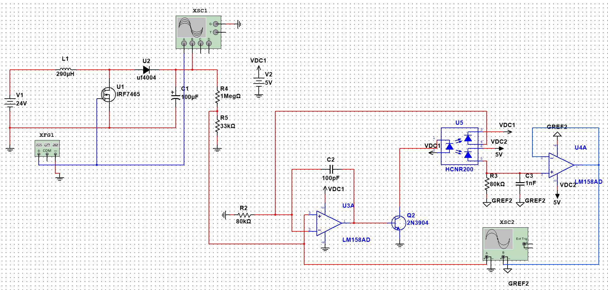
Then I added an voltage measurement circuit for the microcontroller's ADC. It uses voltage divider R4 R5 to bring 24-100 V to 0-3.3 V, which can be read with the MCU, and a linear optocoupler HCNR200 for galvanic isolation. enter image description here enter image description here Simulation seems to be working, but I'm still not sure that it would work in real life. So here is a few questions:
  1. Am I on the right track with the approach I've taken for creating a boost converter controlled by an STM32?

  2. Is there any way to limit the maximum voltage to 100 V? Because adjusting the voltage with ADC feedback doesn't seem too reliable.

  3. Are the chosen values for the voltage divider appropriate, or should I reevaluate them?

  4. Is the PWM frequency value of 100 kHz is ok for my purposes? And how to choose it properly?

Any feedback will be appreciated!

\$\endgroup\$
5
  • \$\begingroup\$ From your description it sounds like you not only want to boost the voltage, but also monitor it. I think you're on the right track but I'm thinking of a way that you can monitor your voltage. That's going to be a challenge. A voltage divider could work but the accuracy is not going to get very desirable results because you're squeezing 100V to fit inside of a 0 to 3.3V measurement scale. \$\endgroup\$
    – Colin
    Commented Mar 15 at 0:54
  • \$\begingroup\$ I would consider starting with a proven boost converter circuit and then using the PWM signal to distort the feedback. \$\endgroup\$ Commented Mar 15 at 2:15
  • 2
    \$\begingroup\$ figure 1 seems to be missing any load on the converter output, did you test the converter under the expected load? \$\endgroup\$ Commented Mar 15 at 2:17
  • \$\begingroup\$ I tested the converter with a 1k resistor as a load since 100V/100mA=1kOhm. It is not on the figure, as I took the screenshot after adding the voltage divider. \$\endgroup\$
    – Dmarm
    Commented Mar 15 at 5:45
  • \$\begingroup\$ regarding pwm as feedback, this requires a voltage to frequency converter, right? What is the advantage of this approach compared to measuring voltage using an ADC? \$\endgroup\$
    – Dmarm
    Commented Mar 15 at 5:48

2 Answers 2

1
\$\begingroup\$

Is there a reason to use the STM32 to drive the converter?

Most converters have a model of the instantaneous inductor current and then control the current cycle by cycle. They typically measure the current by measuring the voltage across the power FETs during the active phases, but with some complex rules to blank off the initial high values seen due to ringing, etc.

A voltage-only feedback cannot know how much current is flowing in the inductor. Imagine the output is shorted. How do you avoid driving the inductor to saturation/destruction?

You end up having to design it so that even in the worst case the inductor current is discontinuous (meaning it is guaranteed to return to 0 at the end of each cycle). Now you can use a software model of the inductor to predict peak current based on pwm duty cycle. But when you try to do this you will severely limit your maximum duty cycle.

That means high power and expensive inductor and lots of ripple.

It's cheaper and more reliable to use an off the shelf boost converter that can achieve your 100V output using a smaller inductor (higher switching frequency) and then bias the switcher's FB pin to push the voltage up and down. You make the bias dynamic by using a pwm output as a DAC that feeds into a resistor connected to the FB pin.

Design it so that with the PWM output at 0v (0% duty cycle) the output is 100V. Then as you ramp up the duty cycle the FB pin voltage should increase and the switcher will lower the output voltage in order to return FB to the nominal reference voltage.

If you need galvanic isolation choose a switcher that supports that.

Do you actually need to know the actual output voltage in the stm32? If not, you can just assume that it is whatever it should be based on current pwm output. If you do, then you can measure the voltage at the FB pin via a buffering opamp. You can compute the actual voltage from the voltage at this node, assuming you know what the PWM output voltage is.

\$\endgroup\$
2
  • \$\begingroup\$ Thanks for the explanation! Now it's a bit clearer to me that it would be quite difficult to foresee everything and it's better to use a ready-made converter. Do I understand correctly that for this I should take a boost converter (LT8361HMSE seems to fit) and feed the FB pin of the PWM through an RC filter, setting the reference voltage? \$\endgroup\$
    – Dmarm
    Commented Mar 15 at 10:36
  • 1
    \$\begingroup\$ You should design the FB circuit according to the datasheet of your boost converter first. That will end up with a resistive circuit feeding the FB node. Now you need to add another resistor that feeds FB node and you need to size that resistor such that it will scale the output between max and min vout as you sweep the DC voltage (basic resistor network analysis). To generate that DC voltage you need to pass the PWM through an RC circuit that removes a much role as possible whilst still giving you the sweep rate you want. \$\endgroup\$ Commented Mar 15 at 10:45
1
\$\begingroup\$

Am I on the right track with the approach I've taken for creating a boost converter controlled by an STM32?

When it comes to digital control of DC-DC converters many different things should be considered.

The idea of taking feedback from the output and adjusting the PWM duty cycle is not enough, but can be just a starting point. As pointed out by Robin Iddon's answer, it's unclear how the core saturation of the inductor L1 will be prevented because you have feedback of neither the load current nor the inductor/switch current. With the switch current information, you can sense and generate response to different loading as well as fault conditions.

Also, note that buffering the output sample before feeding back to the MCU will bring some delay. Depending on the swing/amplitude this can take microseconds (ignoring the ADC measurement delays). So a sudden change on the output voltage (due to a step load change, for example) will be sensed with a delay therefore the response will have a delay accordingly. Although a voltage rise (overshoot) cannot be corrected by anything (i.e. you'll have to wait for it to dampen anyway), a voltage "dip" (undershoot) can still be sensed and "corrected". You may want to re-consider that section if a good dynamic response is a requirement for your application. If you go for a P (proportional) control here, as it's the easiest method, you may end up with a funny output waveform in case of a step load change.

Is there any way to limit the maximum voltage to 100V? Because adjusting the voltage with ADC feedback doesn't seem too reliable.

Limiting the PWM duty cycle in the software may not be enough because you'll need the input voltage information as well (even if you limit the PWM duty cycle, a 1V increase of the input will reflect the output as ~4V). You may want to consider interrupts generated by comparators, for example.

Are the chosen values for the voltage divider appropriate, or should I reevaluate them?

What you should consider is the bias currents of the target (buffer input or ADC). I haven't checked the bias currents of anything on your circuit.

Is the PWM frequency value of 100kHz is ok for my purposes? And how to choose it properly?

This depends on other design details and requirements such as EMI, efficiency, etc. You can choose a higher frequency to make the inductor smaller, but this may bring you trouble with efficiency and EMI, for example. Without knowing other details, it's difficult to answer. But 100 kHz is usually a good starting point.


It might be better to use a boost converter/controller IC and "tweak" externally. I posted an answer here explaining a method. You might be interested. The method employs a DAC but you can make a crude DAC with a PWM + RC filter.

\$\endgroup\$

Your Answer

By clicking “Post Your Answer”, you agree to our terms of service and acknowledge you have read our privacy policy.

Not the answer you're looking for? Browse other questions tagged or ask your own question.