1
\$\begingroup\$

I'm currently designing a carrier board for the Raspberry Pi CM4 that physically includes:

  • 1 Compute Module
  • 2 DF40HC connectors
  • 4 Steel standoffs

I've encountered a dilemma in generating assembly data with a BOM entry for each part. Directly listing each component individually in my schematics has several drawbacks:

With two connectors, I don't have access to the pin name or the correct number. I have to be very careful when routing the PCB to accurately position each of the 6 elements.

To improve this, I considered having one component with multiple parts in my schematics, as shown below. This approach groups pins with their associated functions, enhancing the readability of the schematics. However, it also presents challenges:

From the PCB perspective, this appears as a single footprint, complicating the division of the BOM into 6 distinct elements.

During assembly (handled by Eurocircuits), it would be difficult to specify how to assemble the board accurately.

What alternatives or solutions are available to address these problems, ensuring both schematic clarity and BOM accuracy?

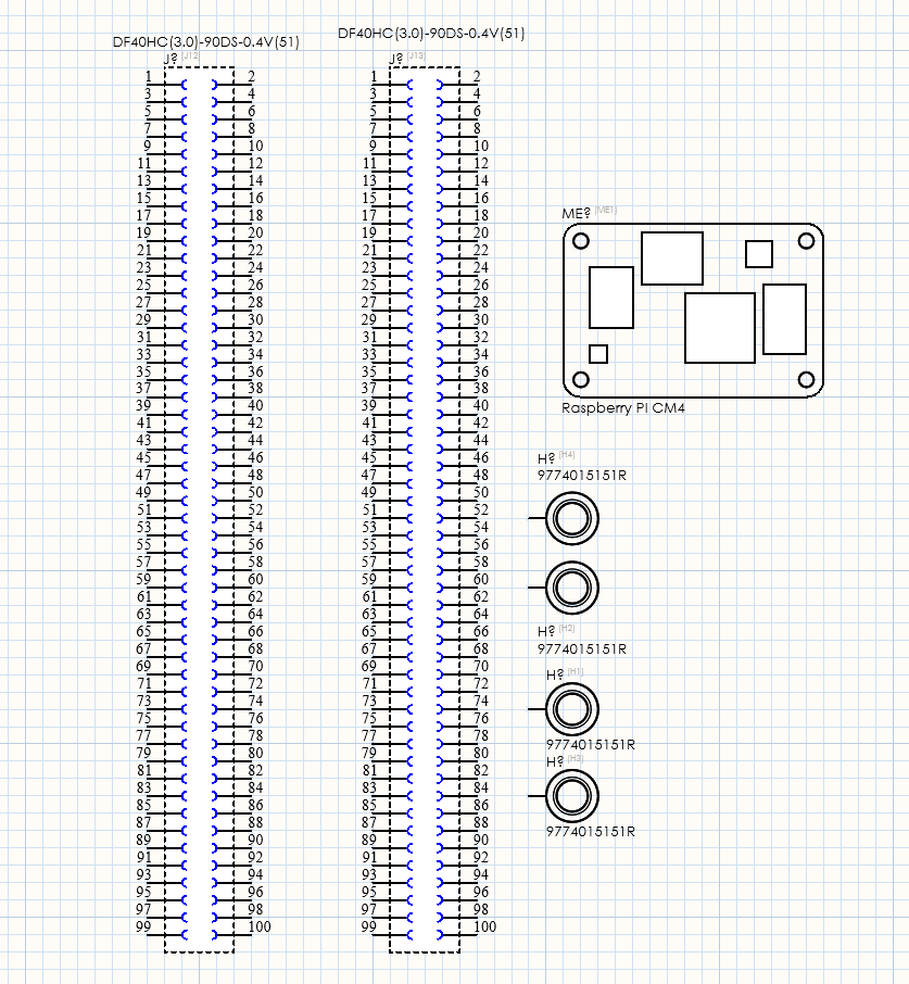
First solution

enter image description here

Second solution

enter image description here

\$\endgroup\$
0

1 Answer 1

1
\$\begingroup\$

What alternatives or solutions are available to address these problems, ensuring both schematic clarity and BOM accuracy?
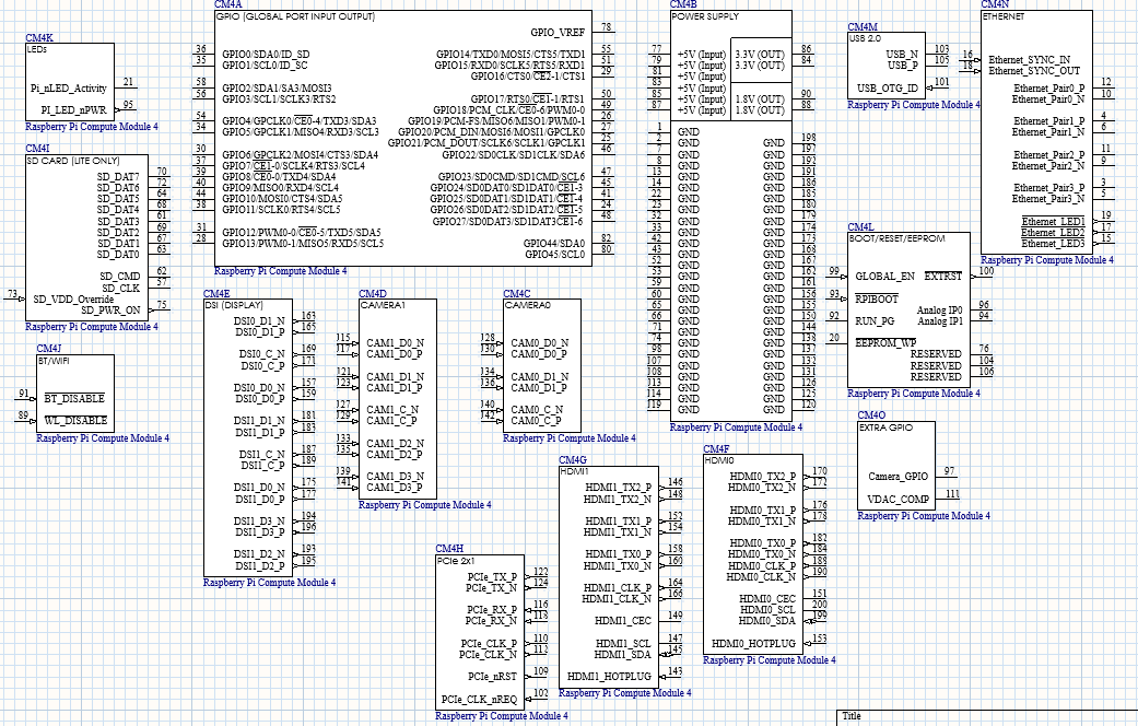
Those two forms of schematic are what I've seen. I don't think there is a way to improve from either of those two.

I usually choose pin connector schematics like the one on the top when I want to refer to the connector and print out the schematics for debugging.

The block diagrams are useful if you want to group pins by function and are more useful for tracking down pin names if you know what it's connected to.

You could do both if you mark one of the diagrams as graphical and then you won't confuse the PCB importer.

\$\endgroup\$
1
  • \$\begingroup\$ None of the solutions works for me. The first one requires each time I use a CM4 to look at the datasheet and position very carefully each element on the PCB. It is an error-prone solution. The second is great, I have one symbol, one footprint. But I cannot use it for assembly because Altium doesn't tell me how to assemble 6 sub-parts at different locations with one physical footprint. \$\endgroup\$
    – nowox
    Commented Apr 3 at 22:30

Your Answer

By clicking “Post Your Answer”, you agree to our terms of service and acknowledge you have read our privacy policy.

Not the answer you're looking for? Browse other questions tagged or ask your own question.