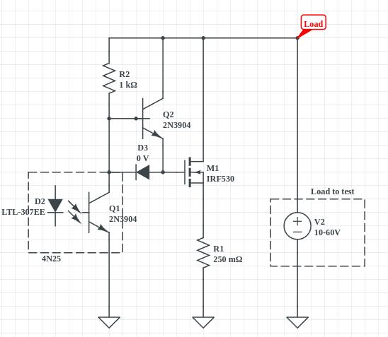
Your question is very vague, and normally I'd ask for more details in the comments. However, there are so many questions, and so many potential flaws in this design, that I'll write an answer addressing the big ones, instead. In that sense it's not so much a solution for you as it is a guide to what you need to fix.
The MOSFET in your design is configured "common-drain", or as a "source-follower", and resistor R1 cannot ever have the full supply (V2) across it. It will always be a few volts short of that. If VG is M1's gate potential, and VGS is its threshold voltage (3V for the IRF530), then voltage VR1 across resistor R1 is:
VR1=VG−VGS
That may be fine, but this arrangement of the MOSFET implies you require analogue control of VR1. Using the 4N25 in an analogue context such as this (without feedback or other means of regulation) will not give you precise or even predictable results.
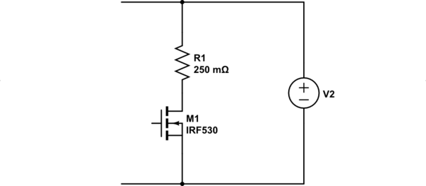
I presume the system is intended to be fully "on or off", digital in nature, for which you will have to connect the MOSFET common-source:

simulate this circuit – Schematic created using CircuitLab
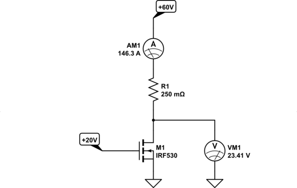
Secondly, the quoted on-state resistance of the IRF530 is 160mΩ, which is comparable with R1 (it's about 60%). This means that even with M1 as "on" as its possible to be, it will have a large chunk of the supply voltage across it, and current will be huge:

simulate this circuit
VM1=VSRM1RM1+R1=60V×0.16Ω0.25Ω+0.16Ω=24V
If your "active load" voltage source has significant internal resistance (compared to the resistances or R1 and M1), then this might too be fine, but these resistances (and the commensurate current) are big considerations.
On top of that, most regular MOSFETs have severe limitations on the magnitude of VGS that can be applied. For the IRF530, (and many, many others), that limit is ±20V, meaning that you can't ever allow gate potential to differ from the source by more than 20V in either direction.
This introduces another problem, which is that with a supply of potentially 60V, whatever portion of that isn't VGS will be dropped across whatever element lies between +60V and the gate. In other words, the potential difference across the gate's "pull-up" element will be:
V2−VGSMAX=(+60V)−(+20V)=40V
This will clearly dissipate a lot of power if there's a lot of current flowing, so you'll need to limit that current somehow. If you wish to avoid heak-sinking of the pull-up element, then you should aim for power dissipation under 1W:
P=I×V=I×40V<1W
I=PV=1W40V<25mA
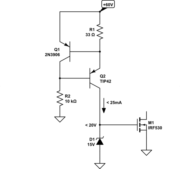
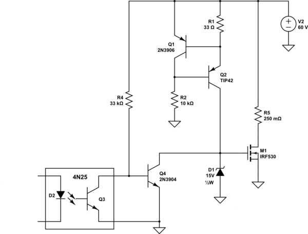
The easiest way to enforce this constraint, that comes to mind, is with a constant current source. I'll employ a zener diode to constrain gate potential to 15V, also:

simulate this circuit
Q1, Q2, R1 and R2 set current through D1 at about 22mA, regardless of supply voltage. This means that pull-up element Q2 and D1 will dissipate less than 1W across the entire voltage range. M1's gate cannot raise above +15V, and so it is also safe.
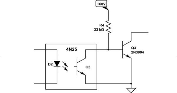
The last element to add is the transistor to pull gate potential to 0V, but it's not as simple as using the opto-isolator's own transistor, since it must pass 25mA or so. The opto-isolator has a current transfer ratio (CTR) of less than 100% (could be as low as 30%), meaning that LED current would have to be well over 25mA to switch the transistor fully on. We'll need another transistor to keep collector current in the opto-isolator reasonable:

simulate this circuit
The 4N25 collector current here is 2mA maximum, requiring about 7mA of LED current to obtain that.
Putting all this together:

simulate this circuit
No promises, I haven't tested it. The folks here will no doubt point out any potential issues.

