Simple question: what do you call this arrangement of mutual-feedback transistors?
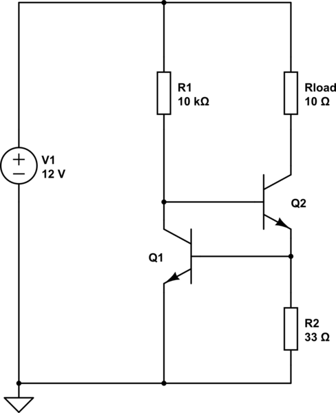
simulate this circuit – Schematic created using CircuitLab
Simple question: what do you call this arrangement of mutual-feedback transistors?

simulate this circuit – Schematic created using CircuitLab
This is a constant current sink. It isn't (to my knowledge) named after its inventor, so sadly there seems to be no moniker that that distinguishes it from other designs. Another user (Hearth) suggested "two-transistor current sink", but your own term "mutual-feedback transistors" could fit the bill too. Perhaps it will catch on.
It may also be referred to as a current limiter (as might any constant current sink/source) because it cannot force current through the load. It cannot prevent a load from passing less current (in magnitude) than the intended amount, but it will certainly impose an upper constraint.
Some might call it a current source, rather than a sink, because people tend to call anything that regulates current a "current source", regardless of whether it sources or sinks, but strictly speaking your circuit is a sink.
That's the simple answer, to your "simple question", but for more details, read on.
In your circuit current is being "sunk" to ground through the 10Ω load. If it were made using PNP transistors instead, then it would perform the exact same function, except it becomes a constant current source in the true sense, shown below right:
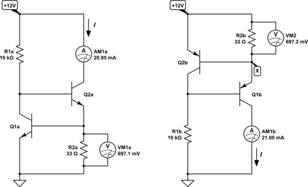
simulate this circuit – Schematic created using CircuitLab
The ammeters are measuring that current \$I\$, which is about 21mA in both cases. We can even insert an extra resistance in that current path (R3 below), and \$I\$ won't change (much), hence my use of the the term "constant":
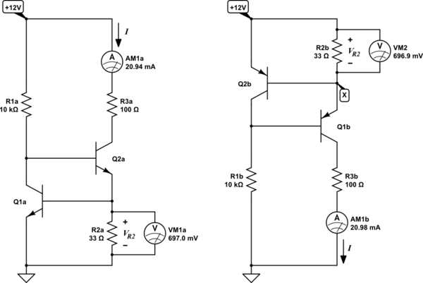
Q2's state is controlled by Q1; If Q1 were to switch off, Q2's base would rise in potential, switching Q2 more on, and vice versa. Q1's state is controlled by the voltage \$V_{R2}\$ across R2, shown on the voltmeters. If \$V_{R2}\$ is more than 0.7V, then Q1 would switch on, switching Q2 off, and if it were less than 0.7V, then Q1 would switch off, turning on Q2.
\$V_{R2}\$ is determined (mostly) by current \$I\$ flowing through R2, by Ohm's law. If you've followed so far, then you can see that when \$I\$ is too much, causing \$V_{R2} > 0.7V\$, then Q2 switches off, reducing \$I\$. Conversely, if \$I\$ is too little, so that \$V_{R2} < 0.7V\$, then Q2 switches on, increasing \$I\$.
In other words, any perturbation of \$I\$ causes the system to react to oppose that perturbation, a kind of negative feedback. The result is that the system settles in the equilibrium condition where \$I\$ is exactly the right amount to produce \$V_{R2}=0.7V\$.
Therefore (approximately, because we haven't accounted for transistor base currents, which are small but non-zero) by Ohm's law:
$$ I \approx \frac{0.7V}{R_2} $$
In the above examples this is:
$$ I \approx \frac{0.7V}{33\Omega} \approx 21mA $$
I took a moment and checked all the references within the time I allowed. Including a book by Linden Harrison called Current sources & Voltage References (Elsevier 2005, ISBN 0-7506-7752-X, PDF at archive.org), which is an historical reference of the topic. The technique using discrete devices for this arrangement appears to have had a very short life-span and, so far as I've been able to find, didn't acquire a recognized name.
Here's a short list of the discrete designs I could find in the literature, starting around 1962 and up to about 1972:
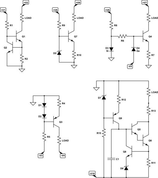
simulate this circuit – Schematic created using CircuitLab
I didn't find acquired names for any of them. Just creativity and publication. There are still more. But integrated circuits took over. It was a creative time. But it was a short time.
I don't have time to fully search the scholarly literature. It's possible that there's a paper somewhere discussing how to design this particular discrete topology well and to discuss physical construction details that may further improve its performance, along with experimental results confirming their approach. But this EESE answer is an attempt worth considering.
There are current mirrors, including a variety of them from Wilson. And Widlar explored more than a few different approaches, including one with beta-compensation and/or with emitter degeneration, all of which probably carry his name. (Those with emitter degeneration would be useful for discrete devices. And I didn't include that one, above.) And finally another developed by Wyatt, while at Honeywell, called a Cascode Peaking current source.
Sorry about not finding a specific name for this one. Perhaps you can interest an historical researcher who specializes in the area of electronic nomenclature.
what do you call this arrangement of mutual-feedback transistors?
Once the current through R2 is sufficient, Q1 starts to activate and keeps the voltage at the base of Q2 at a fairly fixed value. Thus the load (Rload) is fed a reasonable constant current. It's not perfect but, it's good enough depending on your requirements.
So, you ask for a name and I'd call it a low-mid-performance current limiter.
I first saw this beautiful circuit configuration of two interconnected transistors in the output stages of the Widlar's 301 and Fullagar's 741 op-amps as a short-circuit protection; so I suppose it is a Widlar's invention.
It is also used as a current source or a current limiter.
See also What is the idea behind the ingenious Widlar current limiter?
"Ring of two".
That's the most common name I've heard for it. (The rest of this is just waffle to fill for answers' sake...)
AFAIK, it doesn't have a name-name. It might be called descriptively, e.g. "two-transistor current source", in distinction from a "current mirror" which uses two transistors in a symmetrical manner.
It's a simple arrangement; you'd likely have to go back quite far to find a reference. The N-type version could be implemented in vacuum tubes even, though there was little reason to do so, with pentodes available, or with ample voltage to spare to use cathode degeneration and bias voltage for the same purpose. I'd look in Proc IRE in the 1950s (or even late 40s) to see what people were talking about it.
It looks like a current source. The transistor on left \$Q_1 \$biases the resistor \$R_2\$. For small variations in \$R_2\$, current in the load resistor would be constant. If the variation in \$R_2\$ is too great to go into kilo ohms, then current in the load resistor would not be same as in \$R_2\$. It is a not so great but works type of current source.
The other way of implementing this type of current source is to use a Zener diode in place of \$Q_1\$ with its cathode up and connected to the base of \$Q_2\$. This type of current source is actually used in LED lighting where the load would be a LED.
The configuration is also a current limiter.\$Q_1\$ and \$Q_2\$ are biased by the same voltage power supply. Assume \$Q_1\$ conducts low current and the voltage across \$V_{B2}\$ is not high and as a result \$Q_2\$ is off. When \$Q_1\$ starts conducting high current, \$V_{B2}\$ becomes slightly higher, enough to turn on \$Q_2\$ and therefore \$Q_2\$ conducts some current thus limiting the current that flows through \$Q_1\$ reducing the risk that transistor \$Q_1\$ would be burned. This type of arrangement is seen in OP-amps and audio amplifiers.
The circuit is a incomplete arrangement of a safety feature implemented in which the transistor \$Q_2\$ would be protected from over current by making \$Q_1\$ conduct some current.