1
\$\begingroup\$

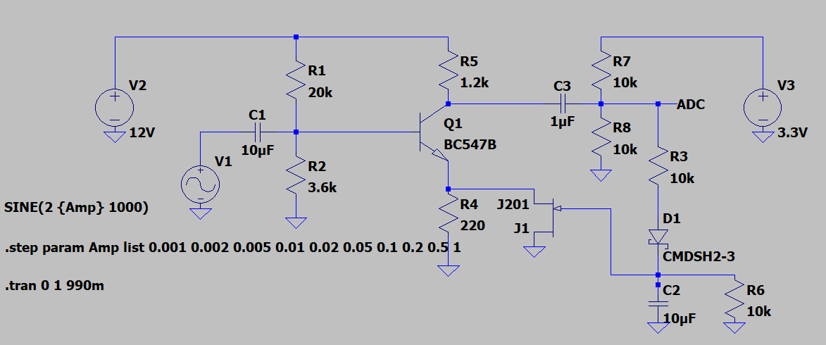
I have been trying and failed. Here I have placed a JFET instead of the second NPN, but it doesn't matter, I just can't fork off enough current from the output into the rectifier and smoothing capacitor.

enter image description here

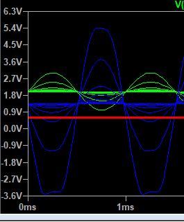
Here are my input wave forms (green) output (blue) and what I get after the rectifier diode (red):

enter image description here

As you can see, there is just not enough juice from the rectifier, and with a lower R3 the output signal is being clipped.

The goal here is to put the output amplitude nicely into the 0-3.3 V range with full swing.

Can it be done? If I need more active components I can just use a MAX9814 and be done with it.

PS: The question was asked if diodes count as active components and let's say for the purpose of this challenge that no, they do not count.

If we have to use a JFET as a variable resistor, we could use the second NPN to amplify the control signal.

\$\endgroup\$
4
  • \$\begingroup\$ The gate / channel diode of the JFET clamps the voltage across C2. The JFET is always conducting and cannot be used this way. Anyway, a resistor parallel to R4 will not properly reduce the gain. \$\endgroup\$
    – Jens
    Commented Nov 21 at 2:19
  • \$\begingroup\$ do diodes count as active components? \$\endgroup\$ Commented Nov 21 at 4:02
  • \$\begingroup\$ why? a bunch of opamps do the work \$\endgroup\$
    – TQQQ
    Commented Nov 21 at 16:25
  • \$\begingroup\$ If AGC is to be applied to an electret microphone, you might try applying a FET AGC at that stage, rather than assuming it is a voltage source and applying AGC at a later stage (as your attempt currently does). \$\endgroup\$
    – glen_geek
    Commented Nov 21 at 16:44

2 Answers 2

0
\$\begingroup\$

Varying the Re (R4) also shifts the DC bias point of Bjt in way the lower R4 the lower Dc voltage on collector.
So you have to adjust DC point so the Vcc limitation doesn’t clamp in widest input signal range. This is adjusted by Rc vs. Re ratio.

\$\endgroup\$
0
\$\begingroup\$

If J1 is an n-channel, depletion-mode JFET, then D1 is backwards and biased incorrectly.

JFETs can have an n-type or p-type channel. In the n-type, if the voltage applied to the gate is negative with respect to the source, the (drain-source) current will be reduced

https://en.wikipedia.org/wiki/JFET - 4th paragraph

To save me a lot of typing, here is a detailed explanation of how a FET works in this application:

https://www.interfet.com/jfet-datasheets/siliconix-an105.pdf

Among other things, there needs to be a coupling capacitor between J1 and Q1 to prevent the changing J1 impedance from altering the Q1 DC operating point.

AND, referring to the post title, a JFET is not a bipolar NPN transistor.

\$\endgroup\$

Your Answer

By clicking “Post Your Answer”, you agree to our terms of service and acknowledge you have read our privacy policy.

Not the answer you're looking for? Browse other questions tagged or ask your own question.