0
\$\begingroup\$

I am currently designing a GaN-based 140W PFC+QR converter, with the QR switching frequency set at 140kHz. While both the PFC and QR sections are operational, I am encountering an issue where the QR side is heating up significantly.

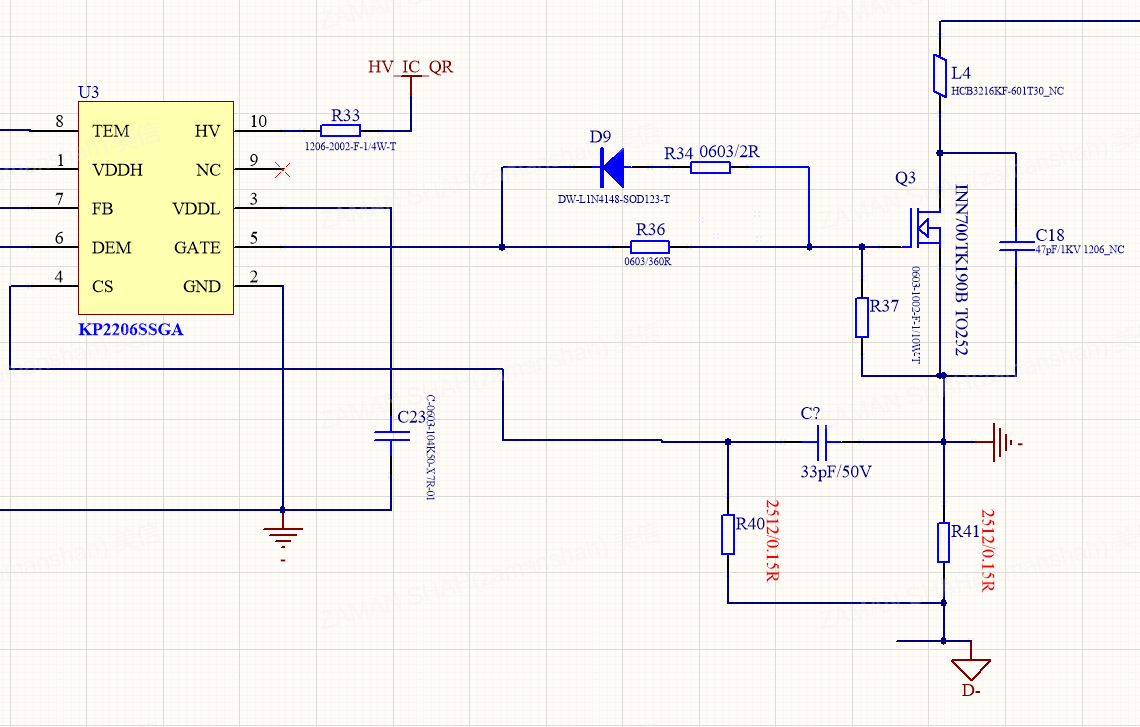
I have attached a screenshot of the QR controller circuithttp://kiwiinst.com/productinfo/1250338.html. My confusion lies in understanding how the current is sensed on pin 9 (CS) of the QR controller. Typically, current sensing is done using a sense resistor (Rsense) followed by an RC filter, but the method used here seems different, and I am unsure if it is correct.

Additionally, I am using a gate resistor (R36) of 360 ohms for the GaN transistor, I share shematic part. I suspect that this value might be too high, causing the GaN transistor to switch too slowly and generate excessive heat. My colleague suggested lowering the Rg value, but this resulted in very high VDS spikes.

I would greatly appreciate any insights or suggestions on the following points:

The current sensing method used on pin 9 (CS) of the QR controller. The appropriate value for the gate resistor (R36) to balance switching speed and VDS spikes. Thank you in advance for your assistance

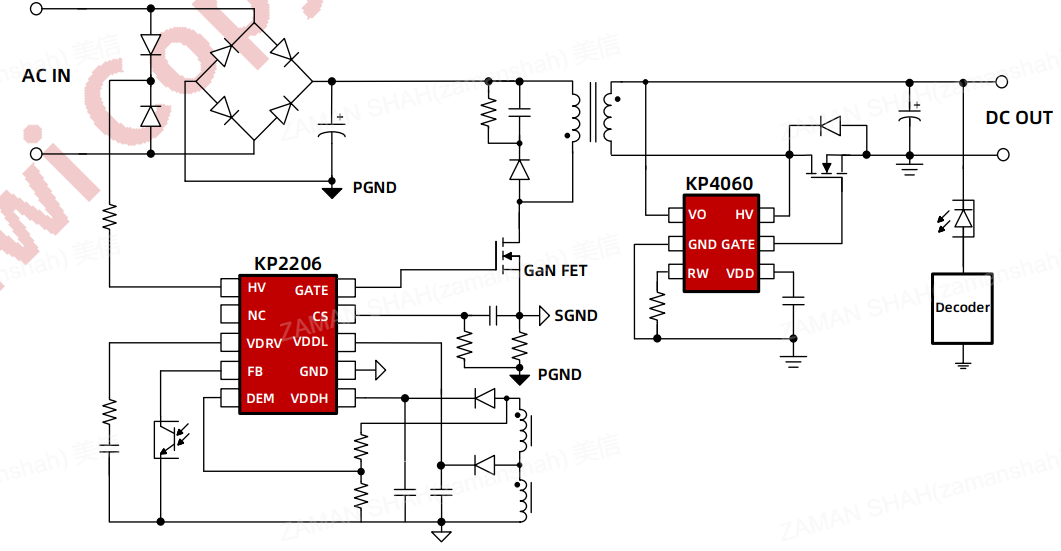
enter image description here enter image description here

\$\endgroup\$
4
  • \$\begingroup\$ GaN needs a large Vgs. What is yours? I suspect that is your problem. Where are your GaN specs? \$\endgroup\$
    – D.A.S.
    Commented 2 days ago
  • \$\begingroup\$ I am using INN700TK190B in datasheet VGS is -1.4V to 7V , and in my circuit VGS is 6V. \$\endgroup\$
    – shah
    Commented yesterday
  • 1
    \$\begingroup\$ First off, when I see a 1-page data-sheet like this one coming from an unknown brand, I stay away from it. There are plenty of well-proven QR controllers from reputable brands, why looking elsewhere? Second, they seem to be using negative sensing, hence the resistance in the return path. If this is popular in CCM PFCs for good reasons, I don't see a justification here for a simple controller. The value you give for driving the GaN looks correct to me but for the drive path, I would suggest to check what the GaN manufacturer recommends. \$\endgroup\$ Commented yesterday
  • \$\begingroup\$ "I've seen GAN recommendations that utilize positive current sensing with the drive path shown in the picture I'm sharing page 16 direct driving section of ynsktmp.workspace23.webfoss.com/uploads/…. However, in my circuit, which uses the same drive path, I am employing negative current sensing. Could this negative current sensing, which introduces resistance in the return path, be causing heating issues? \$\endgroup\$
    – shah
    Commented yesterday

0

Your Answer

By clicking “Post Your Answer”, you agree to our terms of service and acknowledge you have read our privacy policy.

Browse other questions tagged or ask your own question.