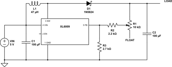
This is a typical boost topology. You can't stop the current to load unless you break the circuit with a relay or MOSFET switch. Enable wont work. When IC is disabled it will not switch and boost voltage, but the input voltage - minus diode forward voltage will still appear at the load. If you look carefully at your schematic you can see that current flows from Vin through L1, D1 and goes to the load no matter if the SW pin of the IC is being switched.
For example if you have 5V input and 12V output, disabling the IC will stop it from switching and voltage at the load will not be 12V, but it will be 5V-0.4V = 4.6V.
The only way to stop it is using a mechanical or semiconductor switch in the current path (input positive or output positive).
UPDATE:
Changing the topology if you will use it only for boost will compromise its efficiency. However depending on your output power and load requirements you could afford a lower efficiency by means of simplicity.
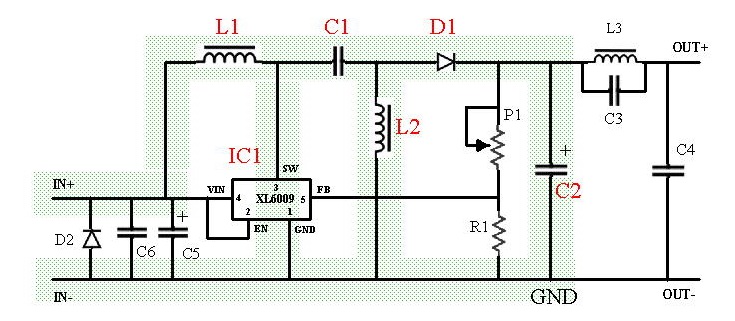
This is a schematic of a buck-boost module which is very popular. If you need a couple of pieces only for your project you can buy it ready assembled.

As I said, efficiency is lower than pure boost (like 70-75% compared to 80-85%) but using this topology you can take advantage of the "enable" pin. You can tie it with a 10k resistor to GND and place the switch between IN+ and EN. When the switch is turned on there will be +Vcc on EN an XL6009 will operate. When your switch is turned off the IC will stop and transfer capacitor C1 will prevent current flowing from input to output.
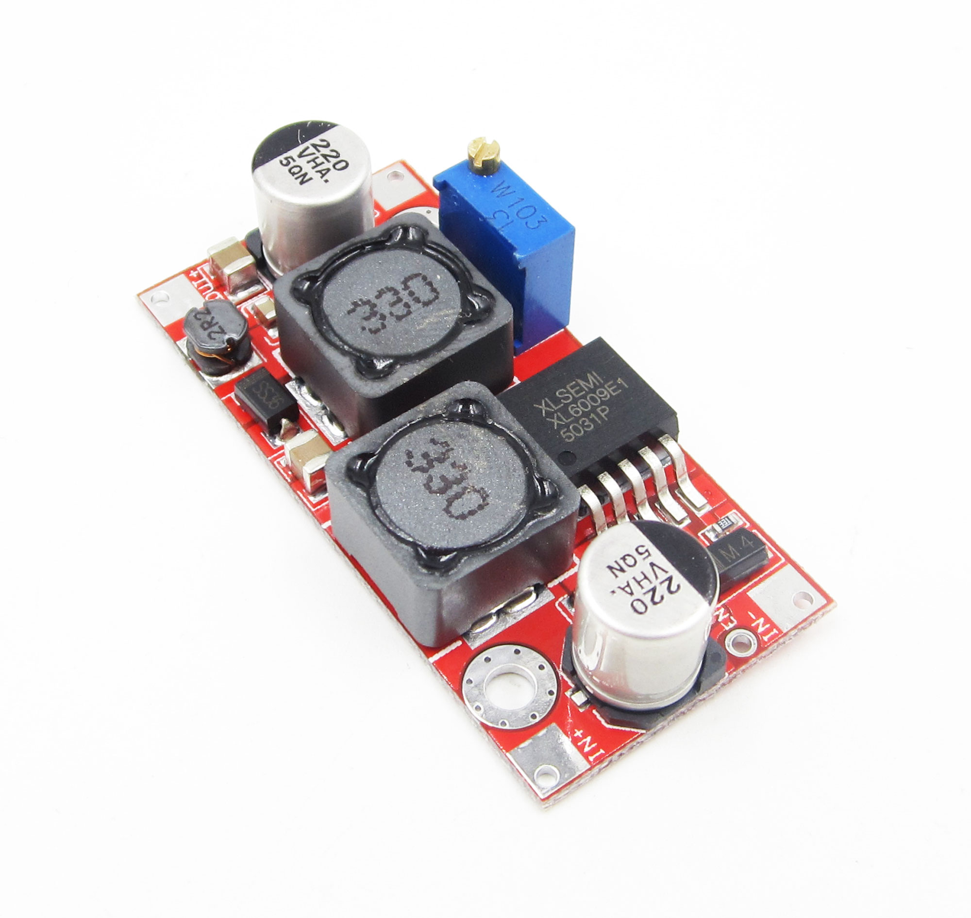
Here is a picrue of a popular module:

The large SMD capacitor between the inductors and schottky diode is this blocking capcaitor.
