1
\$\begingroup\$

The circuit diagram below is given in my book (written by Coughlin and Driscoll).
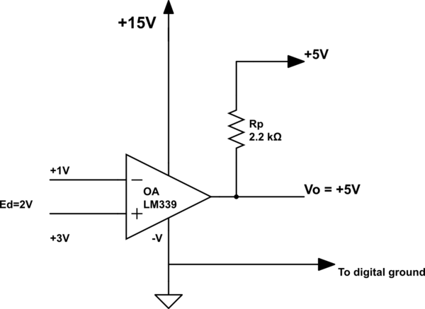
schematic

simulate this circuit – Schematic created using CircuitLab

Here it is said that, at the condition when \$ E_d=+2V\$, the output voltage will be \$V_o=+5V\$. But for an op amp, when the non-inverting voltage is higher than then inverting voltage, the output voltage will be \$+V_{sat}\$, which is approximately +15V.

Why is the output for this Op Amp IC (LM339) +5 Volts?

\$\endgroup\$
1
  • \$\begingroup\$ @What John D said. | With open collector output there is no positive going drive inside the IC - that is provided by the external pullup. In this case they wanted +5V max so used a +5V supply. If they had used a say +12V for the pullup supply it would go to +12V max etc. \$\endgroup\$
    – Russell McMahon
    Commented Aug 14, 2014 at 23:11

4 Answers 4

13
\$\begingroup\$

Well, the LM339 is a comparator, not an op-amp. It is intended to compare the two input voltages and put out one of two levels depending on the result of the comparison. It is not intended to be used with feedback, except possibly positive feedback for hysteresis. The output is an open collector, and there is a pull-up to 5V, meaning that when the non-inverting input is higher than the inverting input the output transistor is OFF, and the output will go to whatever voltage the pull-up (Rp) is connected to.

\$\endgroup\$
2
  • \$\begingroup\$ Oooo... I didn't spot that the 339 is open-collector output. Good eye. \$\endgroup\$ Commented Aug 14, 2014 at 16:33
  • \$\begingroup\$ Good answer +1. It is possible to use an LM339 comparator as a low-frequency op-amp by adding a pullup and external compensation capacitor. See NS AN-74 Fig. 28. \$\endgroup\$ Commented Aug 14, 2014 at 19:49
1
\$\begingroup\$

There is actually a contradiction in the LM339 datasheet:

The output consists of an open-drain NPN (pulldown or low-side) transistor. The output NPN sinks current when the positive input voltage is higher than the negative input voltage and the offset voltage.

vs.

When both IN– and IN+ are both within the common-mode range:

– If IN– is higher than IN+ and the offset voltage, the output is low and the output transistor is sinking current

– If IN– is lower than IN+ and the offset voltage, the output is high impedance and the output transistor is not conducting

TI has confirmed the second case is correct for a similar part here:

https://e2e.ti.com/support/amplifiers/etc_amplifiers__other_linear/f/18/t/631667?LM393-Contradiction-in-the-LM393-data-sheet-

\$\endgroup\$
0
\$\begingroup\$

According to the datasheet,

The output consists of an open-drain NPN (pulldown or low-side) transistor. The output NPN sinks current when the positive input voltage is higher than the negative input voltage and the offset voltage. The VOL is resistive and scales with the output current.

Hence when Non-Inverting(+) is greater than the Inverting(-) terminal the output will be driven to Ground. But when Non-Inverting (+) is less than Inverting(-), the output will be driven to 5V by the pull-up resistor.

\$\endgroup\$
-3
\$\begingroup\$

Given that there's no feedback resistor from the output to the inverting input, the circuit shown SHOULD produce +15V at the output, not +5V; it's acting as a comparator, comparing +1 against +3.

\$\endgroup\$
2

Your Answer

By clicking “Post Your Answer”, you agree to our terms of service and acknowledge you have read our privacy policy.

Not the answer you're looking for? Browse other questions tagged or ask your own question.