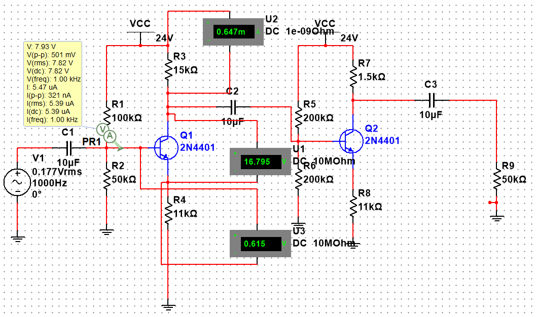
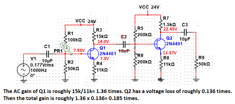
I am trying to design a common-emitter multistage amplifier with gain 40 given \$V_s(t)=0.25\sin(2\pi 1000t)\$ and \$V_o(t)=-10\sin(2\pi 1000t)\$. Vcc is 24v and I want my q-point to be Vce=12v. I have this design, but I don't know where it went wrong.
-
\$\begingroup\$ It's very hard to see what is connected to what, especially around R4. Is R4 shorted out?? \$\endgroup\$– HearthCommented Oct 13, 2023 at 0:37
-
1\$\begingroup\$ @Ma5assik, You aren't going to get an exact gain of 40 without the application of lots of gain coupled with global NFB. Otherwise, all you have is local NFB (emitter resistor) with uncertain attenuation and gains. With part variation it will never be 40. So you really do need a different topology. Also, your base pair biasing is way too weakly handled. But since the topology itself is likely wrong, there's no point fixing that. Also, is your source supposed to have zero impedance? Or is there a source impedance for this project? \$\endgroup\$– periblepsisCommented Oct 13, 2023 at 2:10
4 Answers
I mentioned using global NFB in comments, earlier. I also gather from your approach that you are comfortable with standard CE BJT stages and comfortable with the idea of two such stages. So let's take all these ideas and put them together into a two-stage CE BJT system with global NFB and see if we can get close to what you want to see:
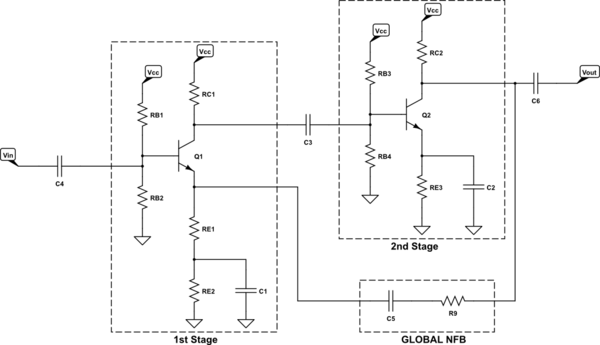
simulate this circuit – Schematic created using CircuitLab
I'm going to make one huge simplification and say that both these stages are biased exactly the same so that their DC quiescent points are identical. The only difference is that in the 1st stage we split up the emitter resistor into two parts, AC bypassing only part of it, while in the 2nd stage we AC bypass the entire emitter resistor. The reason I can do this is that you've not specified a load to drive with the 2nd stage. So I'm free to make this simplification to save some time.
(Completely AC bypassing the emitter resistor is usually a good way to cause substantial distortion of the input source, as the voltage gain varies with the signal, itself. But since this system will be throwing away lots of open-loop voltage gain, using global NFB, this will correct the open-loop distortion and provide a fairly clean output.)
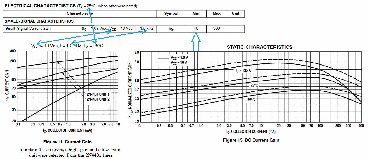
We'll use your \$V_{_\text{CC}}=24\:\text{V}\$ rail, too, and the 2N4401 BJT. The 2N4401 has very poor \$\beta\$ guarantees, as can be seen here from the OnSemi datasheet:
First, let's set all this up to use \$I_{_{\text{C}_\text{Q}}}=1\:\text{mA}\$ per the datasheet's choices -- both the table as well as the center of the x-axis on the charts above. And since Figure 11 claims to have selected a low-gain BJT with \$\beta=130\$ at \$25^\circ\$ and since a glance at Figure 15 suggests we might see \$\frac{.5}{.7}\cdot 170=120\$ at perhaps \$-10^\circ\$, let's go with \$\beta=120\$ as our design number here.
(Hopefully, things only get better with various parts and for temperatures that are above \$-10^\circ\$. Though, technically, I'm still staring at that \$\beta=40\$ figure on the table, too. Up to you how safe you want to be. But for this exercise, I'm going with \$\beta=120\$ in active mode.)
For the quiescent point, I'd want here about \$2\:\text{V}\$ at the BJT emitter for temperature stability. I normally pick something a little smaller (closer to \$1\:\text{V}\$.) But you have a very nice, large \$V_{_\text{CC}}\$. So I'll bite off twice as much to get more thermal stability because I can afford it here.
Since you want \$V_{_{\text{CE}_\text{Q}}}=12\:\text{V}\$, this leaves \$10\:\text{V}\$ across the collector resistor. So that means a DC gain of \$A_v=\frac{10\:\text{V}}{2\:\text{V}}=5\$ for the first stage, ignoring \$C_1\$'s AC bypass effect. But higher once that's taken into account. Meanwhile, the 1st stage is also going to be loaded down by the 2nd stage, so that's going to knock things back down. Let's not worry about all that, just yet.
Some quick calculations give me that the emitter resistor is about \$2\:\text{k}\Omega\$ and the collector resistor about \$10\:\text{k}\Omega\$. A quick skim of Figure 17 (not shown) has me selecting \$V_{_{\text{BE}_\text{Q}}}=650\:\text{mV}\$.
With the rule-of-10 for biasing the base divider pair, and including a little extra for the base current that \$R_{_{\text{B}_1}}\$ must also supply, I find \$R_{_{\text{B}_2}}\approx 26.3\:\text{k}\Omega\$ and \$R_{_{\text{B}_1}}\approx 196.4\:\text{k}\Omega\$. On the E24 table we can find \$R_{_{\text{B}_2}}= 27\:\text{k}\Omega\$ and \$R_{_{\text{B}_1}}= 200\:\text{k}\Omega\$.
\$I_{_{\text{C}_\text{Q}}}\ne 1\:\text{mA}\$, but it will be very close. So we stop here and update the schematic:
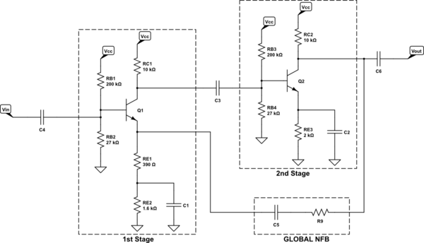
Do note that I split the emitter resistor value (\$2\:\text{k}\Omega\$) into two parts for the 1st stage. \$I_{_{\text{C}_\text{Q}}}\$ will be just a tiny bit higher for the 1st stage than the 2nd stage because I lost \$10\:\Omega\$. But that's only 0.5% change. So no harm here.
Now, it's time we figure out the open loop gain and work out a global NFB figure so that we can specify \$R_9\$.
The expected gain for the 1st stage depends a little on the Early Effect. I don't know exactly what value to pick, though an LTspice model says \$V_A=200\$, which is rather nice. Many have values about half that. Anyway, I'll pick \$V_A=150\$ here just to pick something. This means \$r_o\approx 150\:\text{k}\Omega\$. We also know that \$r_e^{\:'}\approx 25\:\Omega\$. And so the 1st stage's combined voltage gain, taking into account the 2nd stage loading and the 1st stage's Early Effect, gives:
$$A_{v_1}=\frac{10\:\text{k}\Omega\,\mid\mid\,150\:\text{k}\Omega\,\mid\mid\,\left(200\:\text{k}\Omega\,\mid\mid\,27\:\text{k}\Omega\,\mid\mid\,25\:\Omega\cdot 120\right)}{390\:\Omega+25\:\Omega}\approx 5$$
(Note that since the temperature-dependent part, \$r_e^{\:'}\approx 25\:\Omega\$, is small compared with \$R_{_{\text{E}_1}}=390\:\Omega\$ that this calculation is relatively temperature-stable.)
The expected voltage gain for the 2nd stage is:
$$A_{v_2}=\frac{10\:\text{k}\Omega\,\mid\mid\,150\:\text{k}\Omega}{25\:\Omega}\approx 375$$
(Note that since the temperature-dependent part, \$r_e^{\:'}\approx 25\:\Omega\$, is the entire divisor then it follows this calculation is highly temperature-dependent! Over the range of \$-10^\circ\$ to \$+45^\circ\$ this will vary from about 340 to 410.)
Combined, we'd expect an open-loop gain of:
$$A_{v_\text{open}}=A_{v_1}\cdot A_{v_2}=5\cdot 375=1875$$
(But keep in mind that this is a mostly temperature-dependent value. Over the range of \$-10^\circ\$ to \$+45^\circ\$ this will vary from about 1711 to 2065.)
From the standard NFB equation:
$$A_{v_\text{closed}}=\frac{A_{v_\text{open}}}{1+NFB\cdot A_{v_\text{open}}}=40$$
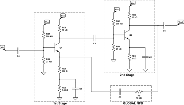
From the above, we'd find that \$NFB=\frac{367}{15000}\approx 0.02447\$. Driving into the \$390\:\Omega\$ AC emitter resistor of the 1st stage, \$R_9=15.55\:\text{k}\Omega\$ (covering the entire temperature-dependent span of \$A_{v_\text{open}}\$):
solve(Eq(solve(Eq(av/(1+av*x),40),x)[0],390/(x+390)),x)[0].subs(av,1875).n()
15550.0544959128
solve(Eq(solve(Eq(av/(1+av*x),40),x)[0],390/(x+390)),x)[0].subs(av,1711).n()
15583.4290843806
solve(Eq(solve(Eq(av/(1+av*x),40),x)[0],390/(x+390)),x)[0].subs(av,2065).n()
15518.1481481481
Looks fairly stable over temperature. So we'll round that up to \$R_9=16\:\text{k}\Omega\$.
(Increasing that value slightly means a little less global NFB and therefore we predict a closed loop gain that will be slightly higher, instead.)
So the final schematic is:
That's it.
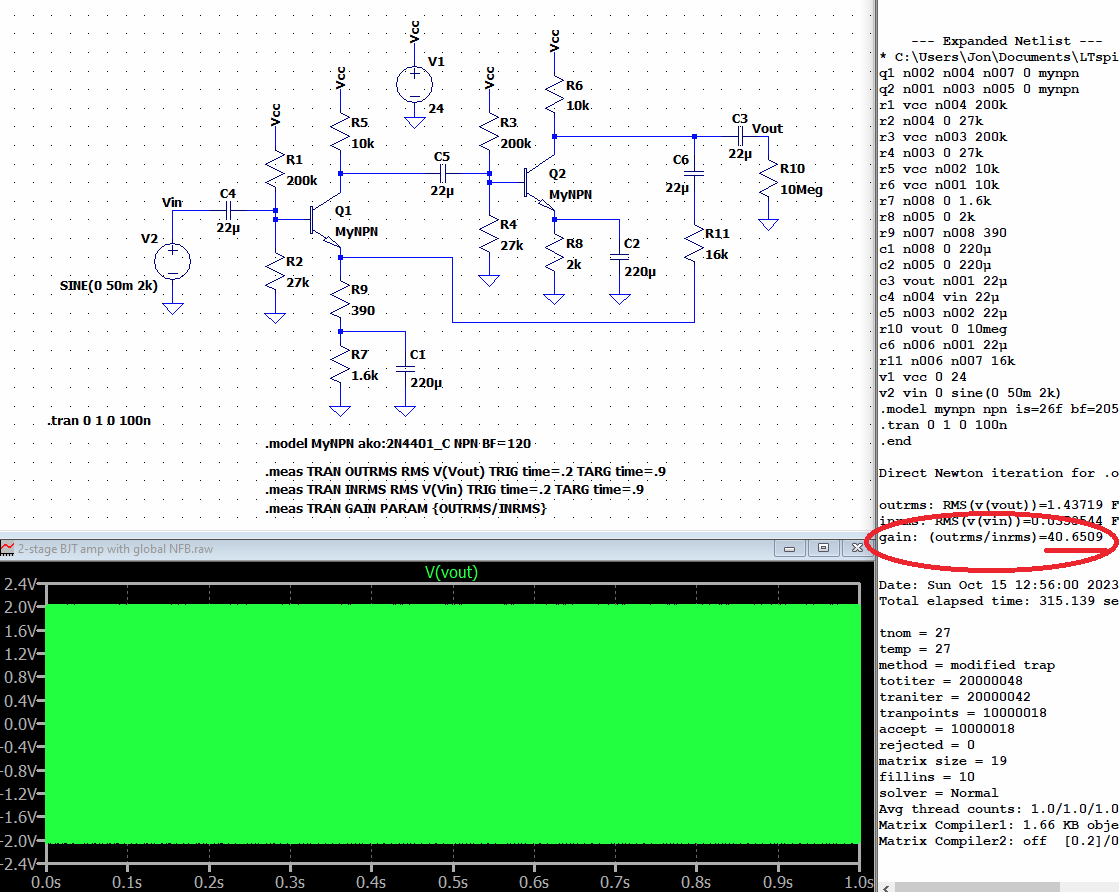
Now, I've honestly not attempted this in LTspice, yet. So I'm going to quickly dash it in and see what happens. With a predicted/designed closed loop \$A_{v_\text{closed}}=40\$, let's set the input signal to a peak of \$50\:\text{mV}\$. This should yield a peak at the output of \$2\:\text{V}\$. Safely within the output compliance range, but also sufficiently visible.
I'll also pick \$f=2\:\text{kHz}\$ and set up some capacitor values that shouldn't interfere too much. The input source will have no source impedance (so I don't need to account for input attenuation) and the output load will be very high (so I also don't need to account for output load attenuation.) This will let us see how close I got in the above estimations and application of the global NFB to control the resulting closed-loop output voltage gain.
Finally, I'll set up some internal Spice measurement tools so that Spice itself will directly perform a gain calculation for me.
Note that the output trace looks about like we expected and that LTspice calculated a gain of \$A_{v_\text{closed}}=40.6509\$ (over on the right, circled and underlined in red color.)
I'm happy with both the process I followed and the results.
Some added thoughts. I ran this at LTspice's default temperature of \$27^\circ\$. Let's see what happens at \$-10^\circ\$ and at \$+45^\circ\$. When performing these runs I get \$A_{v_\text{closed}}=40.4976 \$ at \$-10^\circ\$ and \$A_{v_\text{closed}}=40.7071\$ at \$+45^\circ\$.
So, the gain is pretty stable over temperature, too. Such is the power of global NFB!
Now, I could just as well have chosen to change up the 2nd stage. I may have needed to do so, depending upon the load that needed to be driven. But since no load was specified, I had no specific reason forcing my hand and it was therefore lots easier to just DC bias the CE stage once and copy it into both stages.
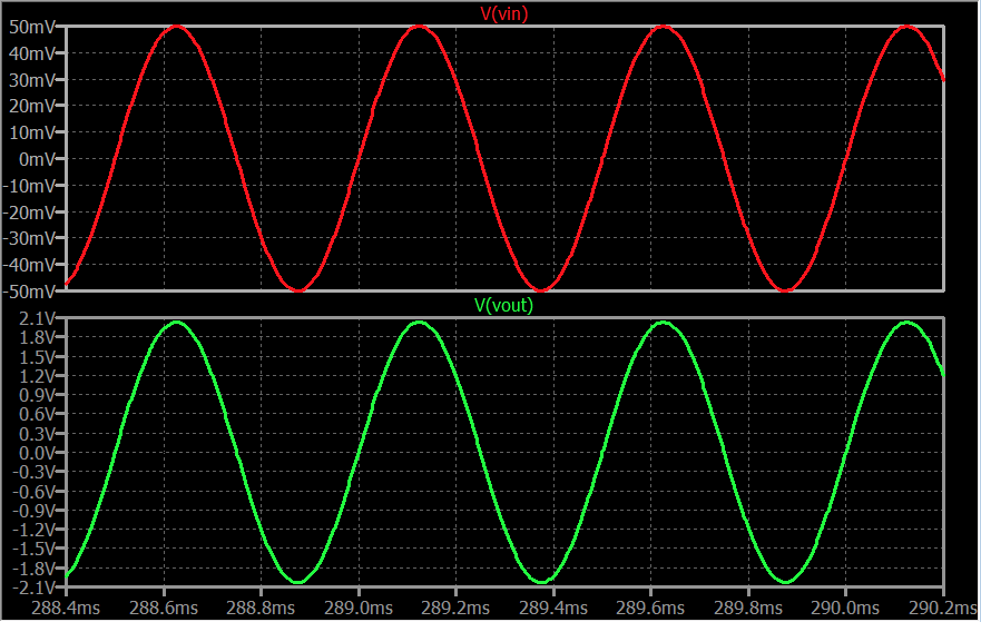
As a final check, let's have a look at the AC output to see if there's any obvious distortion. Remember that I mentioned that completely bypassing the emitter in the 2nd stage might have resulted in distortion, except for the use of global NFB. So let's check to see:
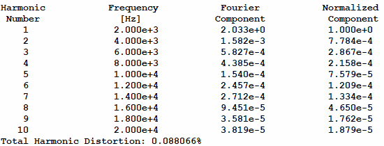
Doesn't immediately look bad. But what does LTspice say, quantitatively? Well, running a .FOUR card for the first 10 harmonics, I find:
A THD of less than 0.1% is pretty good. Nothing to complain about.
If you haven't gotten the point by now, then let me put it in crystal clear words. Create as much open loop gain as you can manage and then throw away most of it with global NFB in order to set the gain you actually want and to reduce harmonic distortion to a reasonable minimum!!!
This is what makes opamps so wonderful! Huge open-loop gain and feedback arrangements you design in order to get what you need.
Isn't it cool how all this works?
-
1\$\begingroup\$ @Carl You want and need as much open loop gain as you can possibly manage. Did you notice that i almost managed to get 2000? It's important! The reason for lower gain in the first stage is that i needed some finite and temperature independent resistance at AC against which to apply the global NFB. If I had also fully bypassed the first stage then I could not have managed temperature independence. So the first stage had to be handled this way. I could increase its gain somewhat but I'd pay for that in making the closed loop gain more dependent on temp. Trade-offs. \$\endgroup\$ Commented Oct 16, 2023 at 8:29
-
1\$\begingroup\$ @Carl This isn't the better topology, though. The only reason i selected if is because of the questioner being more familiar with these CE structures. (And my desire to copy the DC biasing twice.) Otherwise, I'd use the structures found in opamps, which provide far far greater open loop gain and far far better performance. \$\endgroup\$ Commented Oct 16, 2023 at 8:37
-
1\$\begingroup\$ @Carl One last detail. The open loop gain is, itself, temperature-dependent. Especially that of the 2nd stage! So the 1875 varies with temperature. But if you plug in varying values here for the Avclosed = Avopen/(1+Avopen*NFB) equation, you'll find that it is remarkably stable over variations of Avopen. So the overall system is gain-stable over temperature, despite the fact that the open loop gain itself varies somewhat with temperature. Global NFB is a very, very powerful tool. \$\endgroup\$ Commented Oct 16, 2023 at 8:51
-
1\$\begingroup\$ Thanks for the details periblepsis! \$\endgroup\$– CarlCommented Oct 16, 2023 at 9:03
-
1\$\begingroup\$ @Carl Thanks for the kind words. One of the benefits of BJTs over FETs is that they have significantly higher gm. Another is that their 'gate voltage' is a lot lower, so they can work well with lower Vcc. But of course they also have their problems -- notably their recombination base currents. \$\endgroup\$ Commented Oct 16, 2023 at 9:09
I have this design, but I don't know where it went wrong.
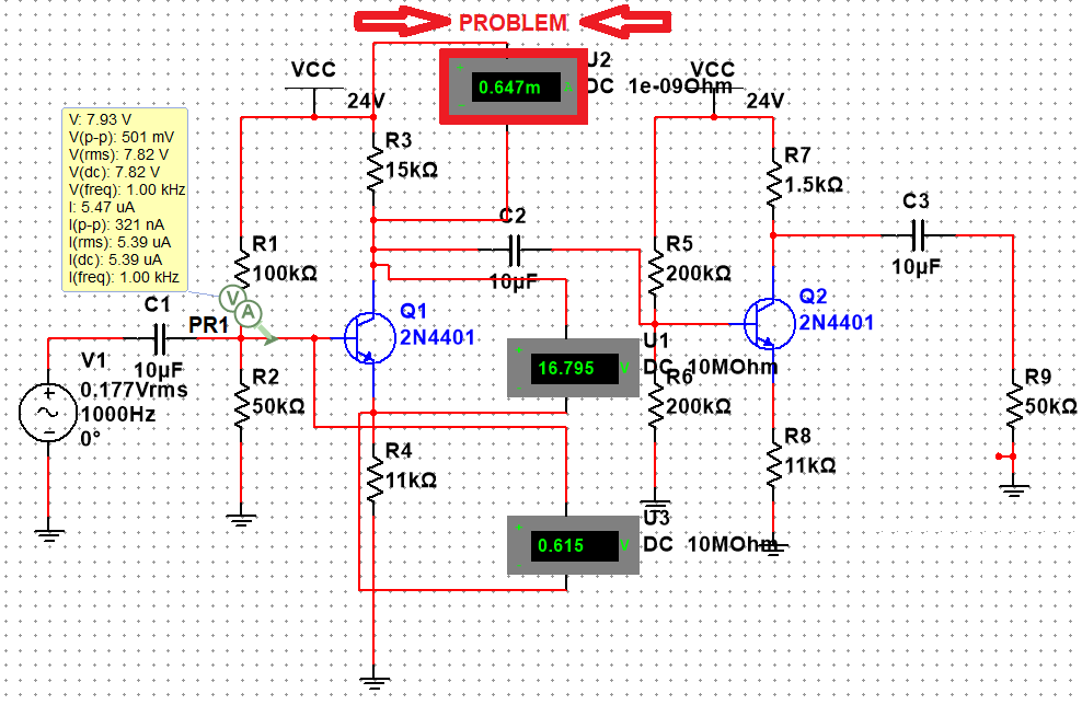
See the problem indicated below: -
Basically, you have shorted out R3 with an ammeter. If you want to measure current, the ammeter goes in series with the component.
There may be other issues but, that one stands out as the most significant.
Remove troublesome ammeter.
Set gain = 40 by setting gain of first stage R3/R4 = 8 and gain of second stage R7/R8 = 5.
Bias the bases so that you get approx 1.5 V across R4 and approx 2.4 V across R8 bearing in mind that there is approximately 0.7 V drop from base to emitter.
Size the base bias resistors such that the current through them is approx 1/10 the magnitude of the emitter and collector currents (which are approximately equal to each other).
The collectors should both now be biased to approx 12 V.
The two gains of R3/R4 and R7/R8 are an approximation and, in practice, they are reduced below these values because of the loading on each stage. The load on the first stage is the input resistance of the second stage and the load on the second stage is R9 (50k). The load on each stage appears in parallel with its collector resistance thereby reducing the gain.
A second approximation I have made is by ignoring the intrinsic emitter resistance re' which appears in series with the emitter resistance RE thereby also reducing the gain below that calculated from my simple gain approximation equations.
Often re' is very small compared to the value of RE and therfore can be ignored when calculating the gain but in a situation where there is only a small amount of unbypassed emitter resistance and perhaps the emitter current is lower in value (making re' larger in value), the value of re' becomes more significant in the gain calculation equation and would then need to be taken into account when calculating the gain.
-
\$\begingroup\$ my professor told us that you cannot multiply both gains from each of the amplifiers, is there another way we can do it? \$\endgroup\$– Ma5assikCommented Oct 12, 2023 at 21:48
-
\$\begingroup\$ @Ma5assik Use one amplifier and partially by-pass the emitter resistance with a capacitor to achieve a gain of 40. That is two emitter resistors in series one of which has a capacitor across it. This is a technique used to achieve a larger gain whilst leaving the dc biasing conditions unaffected. \$\endgroup\$– user350400Commented Oct 12, 2023 at 21:54
-
1\$\begingroup\$ @MaSassik of course, you can multiply both gains - however, the gain of the first stage must be computed taking the finite input impedance of the 2nd stage into account. \$\endgroup\$– LvWCommented Oct 13, 2023 at 7:08

