The power of functional explanations
Why is the collector current in an NPN transistor in CE mode almost independent of the collector-emitter voltage?
In addition to explaining this phenomenon through semiconductor theory (which would do a good job, for example, to take the exam in this subject) we also need a more general functional explanation to imagine what the transistor actually does when it keeps the current constant. In practice, it is what we use to understand circuits (as, for example, the driver does not calculate the trajectory of the car, but somehow intuitively turns the steering wheel as it should). So why dismiss it as "unscientific" when it is what we do our job with?
The advantage of the "functional explanation" is that it captures the most essential idea in the observed phenomenon and is therefore universal. For example, if we can explain here how a BJT keeps the current constant, then we can explain how a FET does it, or how tubes ever did.
Static resistance
Two centuries ago, Ohm found that...
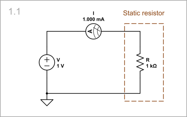
V = 1 V, R = 1 kΩ, I = V/R = 1/1 = 1 mA: ... if we apply a voltage V (1 V) across a resistor with a resistance R (1 kΩ), a current I (1 mA) flows.

simulate this circuit – Schematic created using CircuitLab
V = 2 V, R = 1 kΩ, I = V/R = 2/1 = 2 mA: If we double the voltage (2 V), the current also doubles (2 mA)...

simulate this circuit
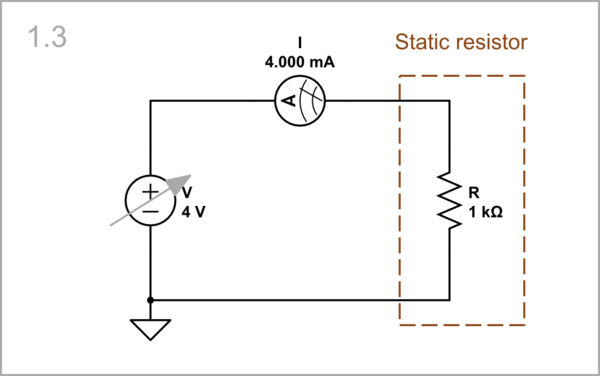
V = 4 V, R = 1 kΩ, I = V/R = 4/1 = 4 mA: ... and so on in the same way (4 V -> 4 mA)...

simulate this circuit
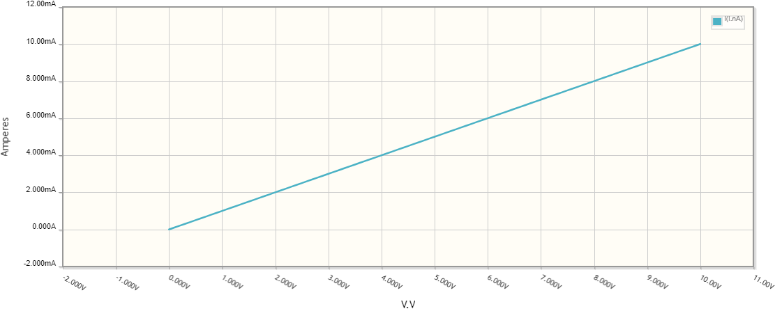
As you can see in the graph below, when you sweep (change) the voltage from zero to 10 V, the current changes proportionally from zero to 10 mA.

So we perceive this resistance as something constant, static, primal... and use it to introduce the next type of resistance.
Dynamic resistance
Now let's imagine that you decided to reproduce Ohm's experiment now, two centuries later.
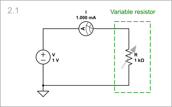
V = 1 V, R = 1 kΩ, I = V/R = 1 mA: For this purpose, you originally set the same voltage V (1 V) across a resistor with the same resistance R (1 kΩ) so the same current I (1 mA) flows. The only difference is that the resistor is variable... but you do not know that.

simulate this circuit
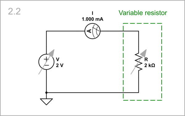
V = 2 V, R = 2 kΩ, I = V/R = 2/2 = 1 mA: Now, when you double the voltage (2 V), I (unnoticed by you) also double the resistance so the current does not change (1 mA)...

simulate this circuit
V = 4 V, R = 4 kΩ, I = V/R = 4/4 = 1 mA: ... and so on in the same way (4 V -> 4 kΩ -> 4 mA)...

simulate this circuit
So you have the illusion that the resistance is infinitely high because the current does not change; the self-changing resistance creates the illusion of infinite resistance.
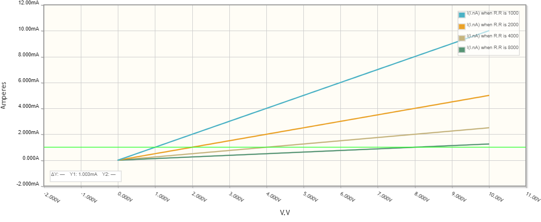
In the graph below, the voltage is swept from zero to 10 V at four values of the resistance - 1, 2, 4 and 8 kΩ. You can imagine that as the voltage increases, the resistor IV curve slopes to the right so that its intersection point with the V IV curve moves along a horizontal line.

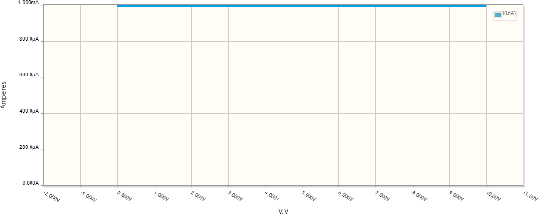
The current (I) does not change because the numerator (V) and denominator (R) of the Ohm's ratio (V/R) change equally. So such a dynamic resistor acts as a constant current source.
Note that "dynamic resistance" is different from "differential resistance". It is a qualitative definition of this type of resistance and literally means "self-changing static resistance"; it serves to understand the phenomena. Differential resistance is a formal quantitative definition and represents a ratio of changes in voltage and current; it serves to calculate.
Conceptual current source
Passive current source
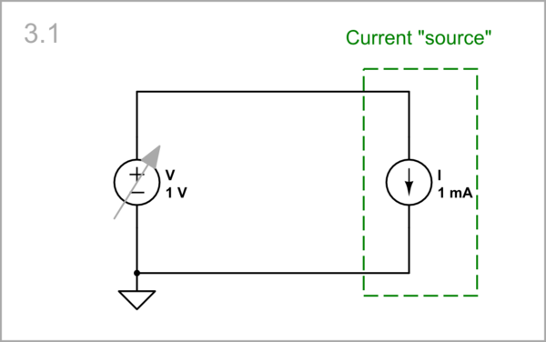
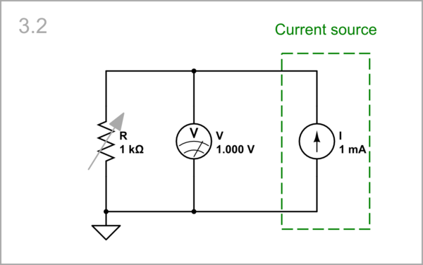
Now we can imagine what might be inside the circle of the current source symbol - a dynamic resistor.

simulate this circuit
When the voltage changes from zero to 10 V, the internal resistance changes from zero to 10 kΩ so the current stays 1 mA.

Active current source
Usually (and here in CircuitLab) it is believed that there is also a voltage source inside. Therefore, we can only connect a resistor to such a "true current source".

simulate this circuit
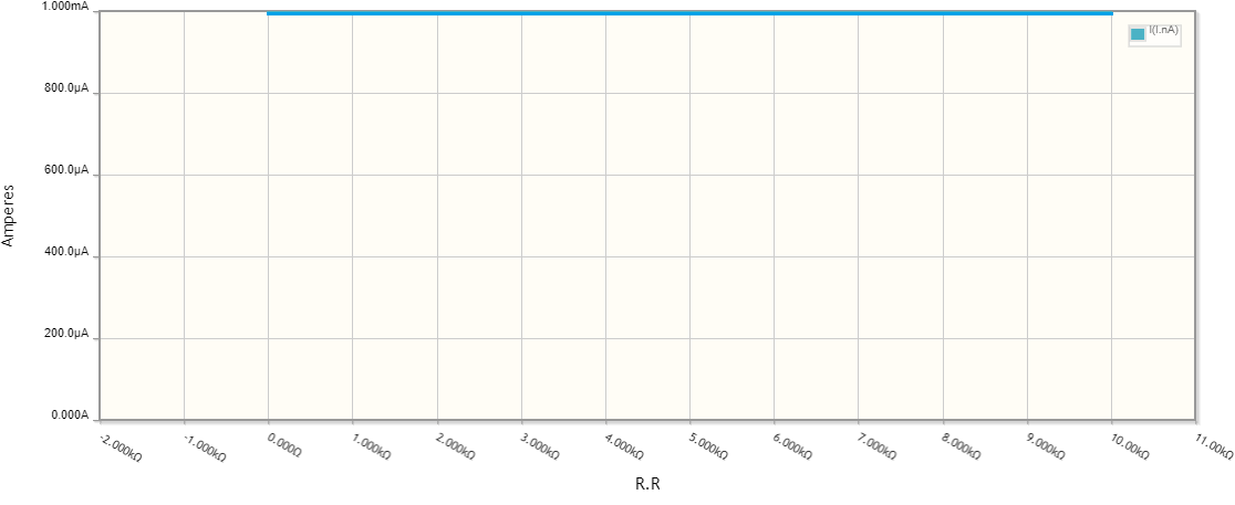
As you can see in the graph below, when you sweep (change) its resistance R from zero to 10 kΩ, the current does not change because the current source decreases its internal resistance (or increases its internal voltage).

Transistor current source
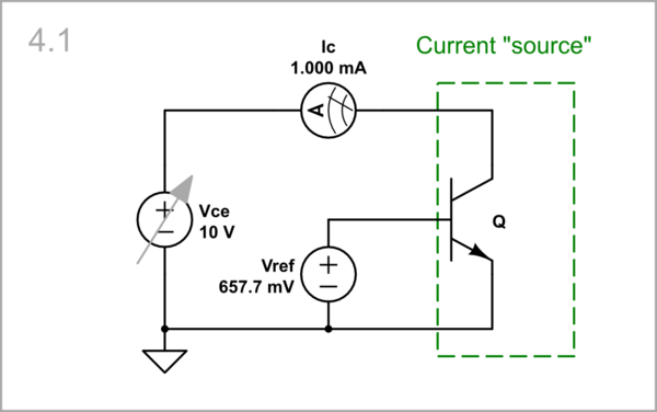
A transistor with constant input (base-emitter) voltage behaves as the dynamic resistor above. It does not contain a voltage source inside; so it is a passive current source. Let's investigate it. Open the Vref parameters window and carefully adjust Vref so that a 1 mA collector current flows (the base current vigorously changes because the base-emitter junction is another type - constant-voltage, of dynamic resistance).

simulate this circuit
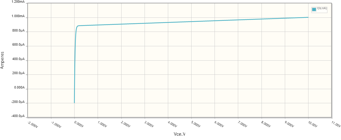
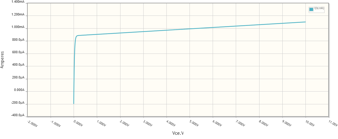
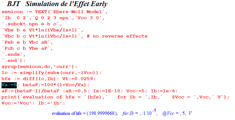
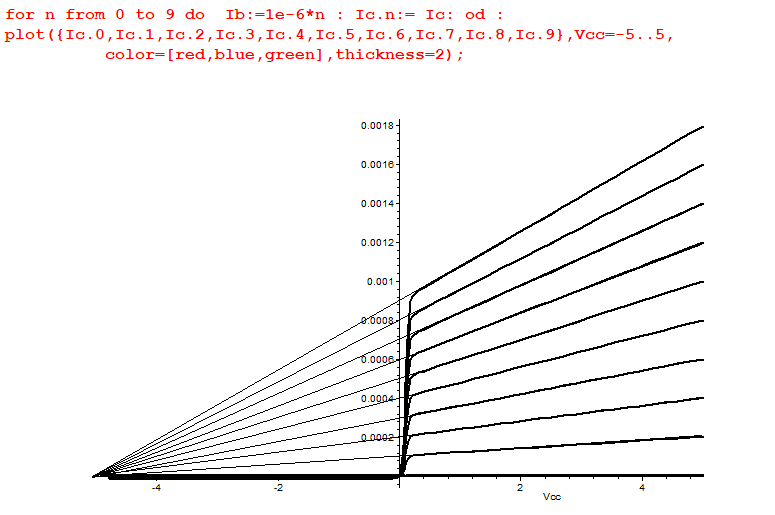
As you can see, it is not a perfect current source because of the Early effect.

Imperfect current sources
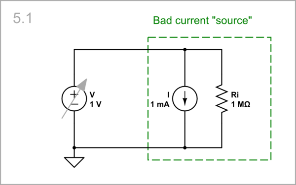
"Bad" conceptual current source
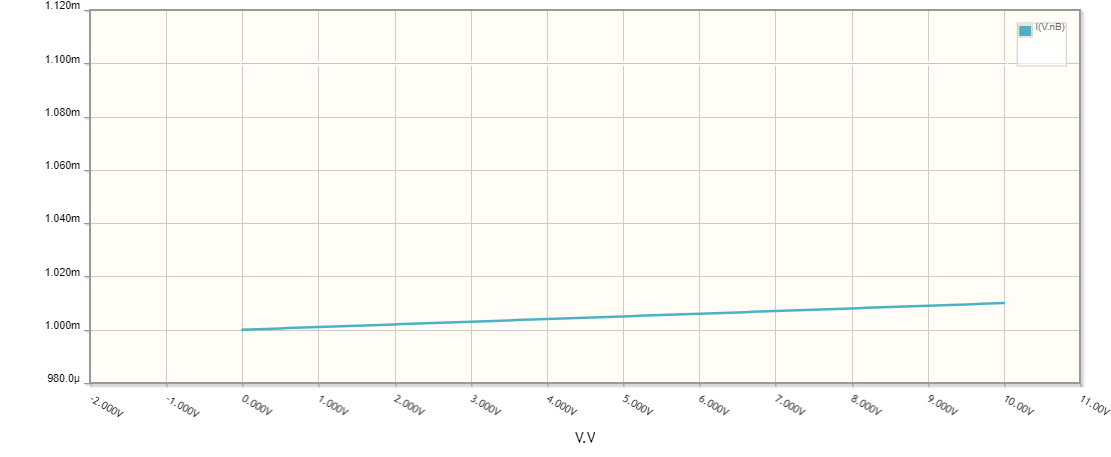
We can simulate this effect by connecting a resistor in parallel to the perfect conceptual current source.

simulate this circuit
We see that the slope of the horizontal part increases.

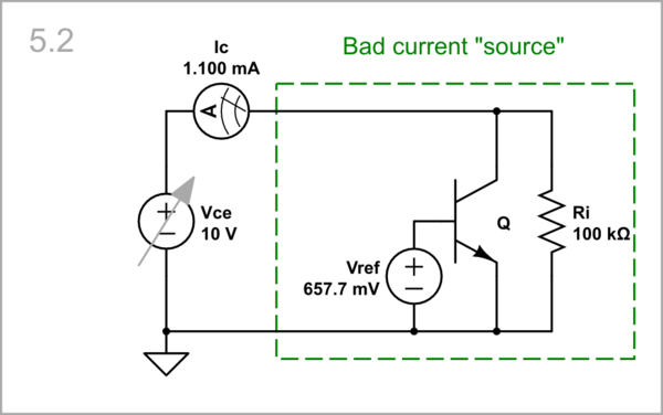
"Bad" transistor current source
We can also connect a resistor in parallel to the collector-emitter part of the transistor...

simulate this circuit
... to "increase" the Early effect.

Conclusions
The BJT collector current is (almost) constant when the collector-emitter voltage changes because the transistor changes its collector-emitter static resistance in the same way.
The transistor behaves as a current-stabilizing non-linear (dynamic) resistor.
The dynamic resistance can be thought of as a "self-varying static resistance".
It is different from the "differential resistance" which is a formal quantitative definition that serves to calculate, and represents a ratio of changes in voltage and current.
See also my Codidact paper.

