1
\$\begingroup\$

I was reading this page about thermal run away.

enter image description here

And it mentions:

Due to increase in the temperature of collector junction, Ico will increase, Vbe will decrease.

But for Ico to increase Ic and Ie, the Ico has to flow through the base-emitter junction and eventually to ground. This would amplify Ico (aka Icbo) and create Iceo = (1+beta) * Icbo.

But all these would happen if R2 would not exist. I mean the above circuit is not the same circuit here.

Since there is R2 which provides a path to ground, would Ico still flow through base-emitter junction or flow through R2 to ground? Because, to me if it flows through R2 it wouldn't cause thermal runaway. (?)

\$\endgroup\$

2 Answers 2

0
+50
\$\begingroup\$

Removing R2 would increase the chances for thermal runaway, there are two "loads" on R1, one is R2 and the other is the transistor. If one "load" is removed than the voltage goes up. If R2 is removed then the voltage Vcb goes up and so does the current Ib. (you could also think of it from a current node perspective and the current through R1 must go through R2 and the transistor, if R2 is removed all the current goes through the transistor, which is a simple way to look at it but it sill works) This would increase current through the transistor because Ib would be higher and so would Ic.

But thermal runaway is independent of this. If you heat up a resistor, the resistance will change a bit (usually in ppm) but this normally doesn't produce a noticeable change in current.

The power dissipated in a transistor is based from Ic. So if you heat up a transistor, you get more current through the collector. This can be bad because this causes the part to heat up more, and more current to flow through, and more heat.

This is why it's important consider the thermal runaway effect and make sure you've considered the changes in beta over temperature. A good idea would to find the max temperature for the design in the datasheet and also consider what would happen if it increased Ic.

Here is an example of how current gain changes in a real transistor with temperature (the 2n3904). At certain currents (like 10mA) Ic would increase with the temperature increasing. The good thing is the designers accounted for the thermal runaway effects and at higher currents, beta/hFE goes down with temperature at higher currents which reduces the thermal runaway effect. In other BJT's, this may not happen. The most important thing is to avoid reaching the absolute maximum temperature of the part.
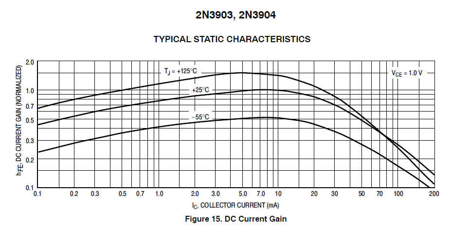
enter image description here Source: https://www.onsemi.com/pub/Collateral/2N3903-D.PDF

Edit:

Since there is R2 which provides a path to ground, would Ico still flow through base-emitter junction or flow through R2 to ground? Because, to me if it flows through R2 it wouldn't cause thermal runaway. (?)

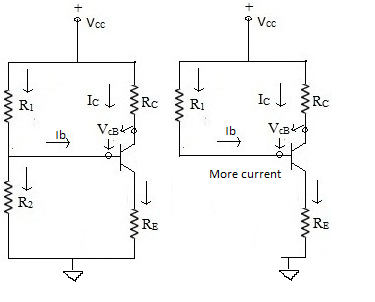
I think the confusion is that for a PNP this would be true, since we have an NPN. If R2 is removed we have more Ib if R1 is the same in both circuits, more Ib means more Ic and more Ie. This would increase the temperature of the part and wouldn't necessarily cause thermal runaway but could cause thermal runaway by starting the cycle. It would depend on the parts in the circuit.
enter image description here

Now if we start from the circuit without R2 adding R2 would decrease the chances for thermal runaway.

No portion of Ie (what you call Iceo) flows through R2 with an NPN. The directions of currents are indicated above.

Since there is R2 which provides a path to ground, would Ico still flow through base-emitter junction or flow through R2 to ground? Because, to me if it flows through R2 it wouldn't cause thermal runaway. (?)

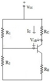
No portion of Iceo flows through R2. All of Iceo flows through Re. All current in a transistor must exit through the emitter.

\$\endgroup\$
11
  • \$\begingroup\$ Please also include where will the Iceo flow through or will it divide between R1 and Re. I cannot find a single source in internet addresses this. \$\endgroup\$
    – pnatk
    Commented May 15, 2019 at 19:19
  • \$\begingroup\$ Sorry, let me clarify, this is an NPN transistor we know this because Re is connected to the emitter. This means that there are two currents that combine to find the emitter currents the equation is Ib+Ic=Ie (which I assume what I call Ie is what you cal Iceo). Iceo goes through Re \$\endgroup\$
    – Voltage Spike
    Commented May 15, 2019 at 19:38
  • \$\begingroup\$ Ib comes from R1 and Ic comes from Rc, the diagram is bad because they don't show Vee or ground on the bottom side and don't show the other currents, but all currents in this diagram will flow through the resistors from top to bottom. \$\endgroup\$
    – Voltage Spike
    Commented May 15, 2019 at 19:39
  • \$\begingroup\$ Adding R2 would decrease the chance for thermal runaway. \$\endgroup\$
    – Voltage Spike
    Commented May 15, 2019 at 19:56
  • \$\begingroup\$ Sadly still not clear because I shouldn't have asked two questions in one. Maybe I shouldn't ask about thermal runaway at all. Lets only focus on the flow path of Iceo. If there is no R2 all the Iceo would flow through emitter resistor. But if there is R2 would all the Iceo flow through R2 or Re or both? I reduced the question to this and if you can answer this it is enough for me. \$\endgroup\$
    – pnatk
    Commented May 15, 2019 at 21:04
1
\$\begingroup\$

R2 doesn't really do anything with thermal runaway. The voltage divider network of R1 and R2 make the voltage bias for the base to emitter junction. When Re is added to the transistor circuit, it controls the base to emitter current to DC ground. Without this, the only current limiting it has is its intrinsic resistance of the junction that defines BetaDC. When the transistor heats up, this resistance goes down, and the betaDC goes up. So it takes a smaller amount of base current to make more current flow in the collector. Putting a current limiting device in the emitter circuit will limit the base to emitter current, and this action prevents thermal runaway. It also (emitter resistor) presents a load for the base to emitter junction so the incoming signal doesn't present an overload condition in the base to emitter junction.

Those papers like that rarely gives you good circuit explanations.

\$\endgroup\$

Your Answer

By clicking “Post Your Answer”, you agree to our terms of service and acknowledge you have read our privacy policy.

Not the answer you're looking for? Browse other questions tagged or ask your own question.