0
\$\begingroup\$

A textbook I use talks about the effects of adding \$R_{E}\$ in a common emitter amplifier. For stabilization of the circuit due to negative feedback

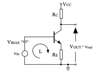
Circuit Image

As the Device gets hotter, more collector current flows, VBE reduces which limits the increase in collector current

What I don't get in this is how when \$V_{BE}\$ reduces this causes a decrease in the collector current as from one of the equations in the textbook $$I_{c}=\alpha I_{E} $$ and $$I_{E}\ =\frac{V_{Bias}-V_{BE}}{R_{E}}$$.

From my rudimentary understanding if \$V_{BE}\$ were to reduce wouldn't \$I_{E}\$ increase which would case an increase in \$I_{C}\$ from the first equation.

\$\endgroup\$
5
  • 1
    \$\begingroup\$ You've included a blank image and haven't asked a question. Please include a proper schematic and tell us what you want to know, and more importantly, what you already understand, about the analysis of the circuit. \$\endgroup\$
    – nanofarad
    Commented Feb 12, 2021 at 23:23
  • 1
    \$\begingroup\$ @nanofarad I've rewritten the whole question, apologies for the 1st mistake it was my first time on this website. \$\endgroup\$ Commented Feb 12, 2021 at 23:27
  • \$\begingroup\$ Read your own quote; it doesn't decrease collector current it; limits the increase. There is a big difference between what the quote says and how you interpret that quote. \$\endgroup\$
    – Andy aka
    Commented Feb 13, 2021 at 10:15
  • \$\begingroup\$ Diztroyer77, Your last equation assumes that IE goes through the base-emitter path only. Hence, no collector current. This cant be correct. Please note that IE is determined by the voltage VBE (Shockley equation) : IE=Is[exp(Vbe/Vt)-1]. It is the small current Is which is temperature dependent. When Is goes high, IE goes high and can be reduced again because the emitter Voltage VE=IE + RE also goes high (VBE goes down because VB=const). See my comment to jonk`s answer. \$\endgroup\$
    – LvW
    Commented Feb 13, 2021 at 11:00
  • \$\begingroup\$ Sorry for the typo: VE=IE*RE. \$\endgroup\$
    – LvW
    Commented Feb 13, 2021 at 15:26

4 Answers 4

2
\$\begingroup\$

With the following circuit:
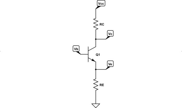
schematic

simulate this circuit – Schematic created using CircuitLab

Assume that \$V_\text{B}\$ is a constant (there's no point confusing the issue by including an AC signal riding on the base's DC setpoint.) What are the variables:

  • \$V_\text{BE}\$ is temperature-dependent and its value may vary by about \$\frac{-2\:\text{mV}}{^\circ\text{C}}\$ for a given collector current. It gets smaller as the temperature rises.
  • \$V_\text{BE}\$ is part-dependent. Different parts from the same bag may have different saturation currents. This alone can be as much as \$\pm 30\:\text{mV}\$, though it is usually not quite that bad.
  • \$V_\text{BE}\$ drifts over time.
  • \$V_\text{BE}\$ depends upon the collector current (which, with an amplifier stage, varies with signal.) So it's signal-dependent, as well, since the signal impacts the collector current -- it must if it is to affect the collector voltage, in fact.

In short, there are lots of things which impact \$V_\text{BE}\$. Over time and place, all of them are involved.

Considering the above circuit, we can treat small changes in \$V_\text{BE}\$ as similar to small changes in an applied signal. If \$V_\text{BE}\$ makes a small change towards getting smaller, this is just like the input signal changing upward and pulling the emitter up. Similarly, if \$V_\text{BE}\$ makes a small change towards getting larger, this is just like the input signal changing downward and pushing the emitter downward.

You'll probably encounter the following closed loop with negative feedback loop from time to time:

schematic

simulate this circuit

Above, B is the negative feedback factor. B is positive when the feedback is negative (per the sign shown at the addition node.) The closed loop gain is \$A_{CLOSED}=\frac{V_\text{OUT}}{V_\text{IN}}=\frac{A_{OPEN}}{1+A_{OPEN}\cdot B}\$. (It's simple to work that out from the above diagram. If you haven't already done so, sit down with pencil and paper and give it a try.)

As you probably already know, the closed loop voltage gain of the above circuit is \$A_v=\frac{R_\text{C}}{R_\text{E}}\$. So we can equate these:

$$\frac{A_{OPEN}}{1+A_{OPEN}\cdot B}=\frac{R_\text{C}}{R_\text{E}}$$

and solve for B:

$$B=\frac{R_\text{E}}{R_\text{C}}-\frac1{A_{OPEN}}$$

Given the Ebers-Moll model for the BJT, we know that \$A_{OPEN}\approx \frac{R_\text{C}\cdot I_\text{C}}{V_T}\$ and also that when \$R_\text{E}\gg\frac{V_T}{I_\text{C}}\$ then \$I_\text{C}\approx I_\text{E}=\frac{V_\text{B}-V_\text{BE}}{R_\text{E}}\$. From these, we can work out that so long as \$\frac{V_T}{I_\text{C}}\ll R_\text{E}\lt R_\text{C}\sqrt[+]{\frac{V_\text{B}-V_\text{BE}}{V_T}}\$ then B is positive and therefore the feedback effect of \$R_\text{E}\$ is negative.

Roughly speaking, for any reasonably design, \$B\approx \frac{R_\text{E}}{R_\text{C}}=\frac1{A_v}\$. So, smaller values of \$A_v\$ imply more negative feedback and therefore more stability with respect to changes in \$V_\text{BE}\$. Another way of putting that is that the more negative feedback you apply, the more stable the circuit is to vagaries relative to variations of \$V_\text{BE}\$ (whether due to temperature, part variation, drift over time, etc.) But also the lower the voltage gain of the circuit. So you make trade-offs. More gain, less stable. Less gain, more stable. It's your call where to place this balancing act.

\$\endgroup\$
3
  • \$\begingroup\$ Hi thanks for the reply it is invaluable, but I still don't understand if VBE were to reduce how it would limit the collector current as from the equation here 𝐼C≈𝐼E=(𝑉B−𝑉BE)/𝑅E wouldn't this imply that as VBE reduces this causes an increase in the emitter current which approximates to an increase in the collector current. Sorry if it's a stupid question. \$\endgroup\$ Commented Feb 13, 2021 at 9:36
  • \$\begingroup\$ @jonk, I have some problems with your feedback model and the corresponding derivations. Quote: "....smaller values of Av imply more negative feedback...". This implies that any change in Rc would change the feedback factor which is not the case. In you model, the feedback factor B is dimensionless, which does not correspond to the real circuit behaviour. Instead, Re causes current-controlled voltage feedback and the feedback factor is beta=RE (of course derived from another model with output=current.). As a consequence, the loop gain is -gm*Re. This has been proven as correct. \$\endgroup\$
    – LvW
    Commented Feb 13, 2021 at 10:10
  • \$\begingroup\$ Here you can find a block diagram which supports and explains th above comments: electronics.stackexchange.com/questions/528064/… \$\endgroup\$
    – LvW
    Commented Feb 13, 2021 at 10:17
2
\$\begingroup\$

If \$I_E\$ increases, \$V_{R_E}\$ must increase.

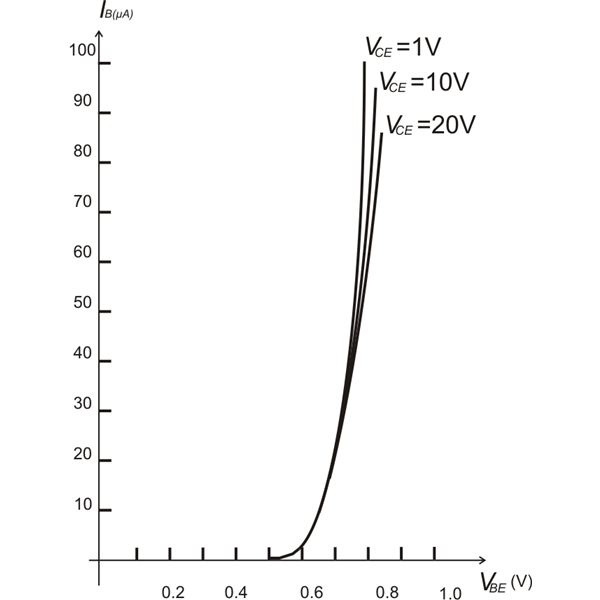
\$V_{\ bias}\$ is fixed, so KVL means \$V_{BE}\$ decreases, which decreases \$I_B\$, which decreases \$I_C\$ and \$I_E\$, stabilizing the Q-Point.

The Q-Point changes, but the addition of \$R_E\$ causes greater stability.

From Input characteristic curve of common collector configuration.

enter image description here

\$\endgroup\$
1
\$\begingroup\$

Adding Re makes the base current more stable by reducing the effects of Vbe(T) ~ -2 to -2.4mV/'C as I=Ve/Re is more stable.

So it reduces the rise of current with rising temperature and lower Vbe, as well as reducing the voltage gain to collector by Rc/Re so this makes it more linear. Adding C across Re, will boost the AC gain for f>1/ReCe

\$\endgroup\$
2
  • \$\begingroup\$ I don`t know how experienced the questioner is - nevertheless, one comment seems to be necessary. When you add a C across Re your formula will result in a signal gain approaching infinity. Therefore, I think it is much more better (and, of course, more correct) to point to the fact that gain=Rc/Re is an approximation only for Re>>1/gm. The correct gain formula is A=- Rc/[(1/gm) + Re] \$\endgroup\$
    – LvW
    Commented Feb 13, 2021 at 9:58
  • \$\begingroup\$ or approx. for C bypassed Re \$ Av=\dfrac{Rc}{(\dfrac{Ve}{0.026*Re} +Re)}\$ Assuming Ie~Ic for \$h_{FE}>>1~ and ~\omega >>\dfrac {1}{ReCe}\$ but I just want to illustrate the reduction of Vbe sensitivity \$\endgroup\$
    – D.A.S.
    Commented Feb 13, 2021 at 13:16
0
\$\begingroup\$

With RE equal to 0 Ohms the collector current is determined by VBE and any small variation in temperature will cause a small variation in VBE (-2.1mV/degC) which will cause a significant variation in collector current and the DC bias at the collector.

By adding RE (emitter degeneration) to the circuit, the collector current is now essentially set by the voltage at the emitter divided by RE and any small variation in VBE with temperature change will have a small effect on VE (relative to its magnitude) and therefore a relatively small effect on IC.

This is the reasoning behind the argument that VE should be at least 1V in a common emitter amplifier so that any small variation in VBE with temperature will cause a relatively small variation of the voltage across the emitter resistor (and therefore the current through it) thereby temperature stabilising the collector current.

\$\endgroup\$

Your Answer

By clicking “Post Your Answer”, you agree to our terms of service and acknowledge you have read our privacy policy.

Not the answer you're looking for? Browse other questions tagged or ask your own question.