5
\$\begingroup\$

I was studying the schematic for the "Waveshare UPS HAT", just because I am a beginner and find it educational. This part is really confusing for me:

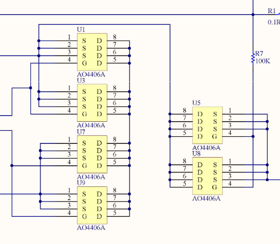
Connected Drains

Why are all the drains of those AO4406A MOSFETs connected together and to nowhere else? What happens there?

\$\endgroup\$
3
  • \$\begingroup\$ I misread your question the first time around. I can't say, without seeing more of the schematic. If you can fit it in, can you revise your question with a schematic that's zoomed out enough to show where the gate and sources are connected, or at least to the point where there's signal names called out? \$\endgroup\$
    – TimWescott
    Commented Apr 3, 2021 at 21:13
  • \$\begingroup\$ @TimWescott Sorry if I didn't make it clear enough. I've linked the word 'schematic' in the first line to the full schematic pdf and thought that would be enough. Do you think I should add the image too? \$\endgroup\$
    – Sohail
    Commented Apr 4, 2021 at 1:24
  • \$\begingroup\$ It's nice to have all the relevant information in the question -- web links rot. Unless it's splattered all over a huge schematic. It ends up being a judgement call. \$\endgroup\$
    – TimWescott
    Commented Apr 4, 2021 at 3:18

2 Answers 2

10
\$\begingroup\$

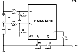
They are connected back-to-back, for different purposes. Charge control, and discharge control. Look up the datasheet for the HY2120 protection IC used, and you will understand how they are used:
enter image description here

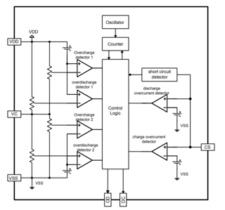
The cell voltages are sensed through the VDD and VC pins, and compared to a fixed voltage. Take a look at this block diagram which is from page 5 in the datasheet.
enter image description here

The 2 FETs M1 and M2 are turned on/off depending on what conditions are met.

M1 connected to the OD pin is turned off when cells is depleted. No current can flow out of the battery but because of the body diode of M1, it can be charged up until it is safe to turn M1 on again and removes the voltage drop from the diode.

The same goes for M2. When the cells is fully charged, M2 is turned off so no more energy can be put into the cells, but the body diode of this device makes sure you still can use the energy from the fully charged cells.

\$\endgroup\$
3
  • \$\begingroup\$ Thank you, that clarifies a lot. But I need more help to understand how that over-charge and over-discharge is sensed through M1 and M2. Can you please explain a little more how that happens? \$\endgroup\$
    – Sohail
    Commented Apr 3, 2021 at 16:36
  • \$\begingroup\$ @Sohail The cell voltages are sensed through the VDD and VC pins, and compared to a fixed voltage. Take a look at the block diagram on page 5. The 2 FETs M1 and M2 are turned on/off depending on what conditions are met. \$\endgroup\$
    – Linkyyy
    Commented Apr 3, 2021 at 18:11
  • \$\begingroup\$ I added some explanation to the answer. \$\endgroup\$
    – Linkyyy
    Commented Apr 3, 2021 at 18:27
0
\$\begingroup\$

Mostly it's for thermal reasons, not electrical. The portion of the transistor that generates the most heat is the drain, followed by the source. On an SO-8 package, the best route for heat out of the chip is the pins, so the drain gets allocated a whole bunch of pins, the source gets almost as many, and the gate gets just one.

If you look at other packages for FETs, like this one you'll see that there's just three connections, but the whole package design is centered around providing a large metal surface area on the drain connection -- this, again, is designed to get the heat out* of the transistor die and onto the board.

* It's certainly not designed for ease of soldering -- trust me on this.

\$\endgroup\$
3
  • 3
    \$\begingroup\$ Tim - Hi, With huge respect, you seem to be answering a different question than the one being asked by the OP. You seem to be answering a question like "why are there multiple drain pins on these MOSFETs" - but that isn't the question, which is: "Why are all the MOSFET drains connected together and to nowhere else?". Do you want to give this answer to that question, as it doesn't actually answer the original question IMHO, despite being interesting in its own right. Thanks! \$\endgroup\$
    – SamGibson
    Commented Apr 3, 2021 at 19:10
  • 1
    \$\begingroup\$ Dangit -- yes, I misread the question. \$\endgroup\$
    – TimWescott
    Commented Apr 3, 2021 at 21:12
  • \$\begingroup\$ @TimWescott I was lucky you didn't down-vote my question since there is already an answered question about MOSFETs with multiple source and drain pins here ;D \$\endgroup\$
    – Sohail
    Commented Apr 4, 2021 at 1:32

Your Answer

By clicking “Post Your Answer”, you agree to our terms of service and acknowledge you have read our privacy policy.

Not the answer you're looking for? Browse other questions tagged or ask your own question.