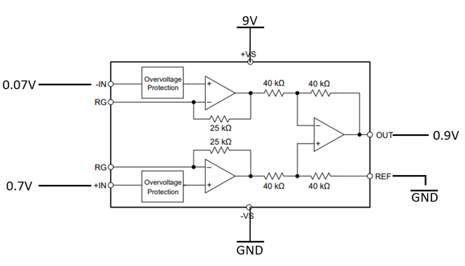
While the datasheet of the INA828 seems ambiguous regarding acceptable input voltage range, it is clear that you can't use inputs so close to the negative rail. The first hint, on page 19 is:
7.3.3 Input Common-Mode Range
The linear input voltage range of the INA828 input circuitry extends within 2 Volts of both power supplies
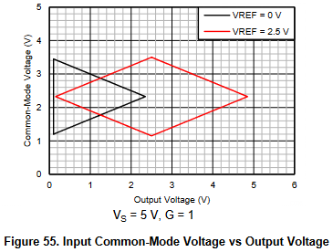
This is confirmed in figure 55 on the same page:

Usually you would be required to set \$V_{REF}\$ to a bias point some point between the supply rails. This makes sense because you usually want the output of a differential amplifier to be able to swing to equal extremes in either direction. You've clamped \$V_{REF}\$ to the negative rail, 0V, so you have constrained yourself to the black region in that graph.
Still, in both curves it can be seen that the boundary of inputs for which the device is expected to operate extends only to within 1.2V of the negative supply, and 1.5V of the positive supply.
The obvious solution to your dilemma is to use a split supply, bringing \$V_S\$ to -1.2V, or more negative. You may still centre the output on 0V by keeping \$V_{REF} = 0V\$.
The graph is confusing, since you would normally consider inputs to be independent (X axis), and output to be the dependent variable (Y axis). However, this graph is intended to describe, for some required output voltage excursion wherein the device is guaranteed to meet its performance specifications, what input voltage range you may use.
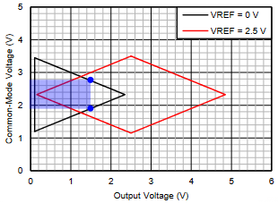
For instance, if you require the output to reach +1.5V, find those points on the graph and project them onto the Y axis, like this:

So, given a 5V supply, and \$V_{REF} = 0V\$, by keeping both inputs within the range \$ 1.9V \le V \le 2.8V\$, and as long as you never expect the output to be less than \$0.1V\$ you can be certain that the output will be correct.
Importantly, this graph also tells you that you can never expect the output to drop lower than 0.1V above the negative supply potential, which makes a single-ended supply absolutely useless if you ever expect the input voltage difference to approach zero! Again, to overcome this constraint, use a dual supply, or alternatively raise \$V_{REF}\$, and use some sort of post-processing to account for the offset.
Be warned - setting \$V_{REF}\$ using a simple potential divider across the power supply will ruin the precision of the output, since the output will then contain whatever noise or regulation error that exists in the supply. For non-zero \$V_{REF}\$, ideally you would use a precision reference.
One of the main reasons for these severe input constraints is that the device uses current feedback (as opposed to the usual voltage feedback) to obtain its otherwise impressive performance.

