5
\$\begingroup\$

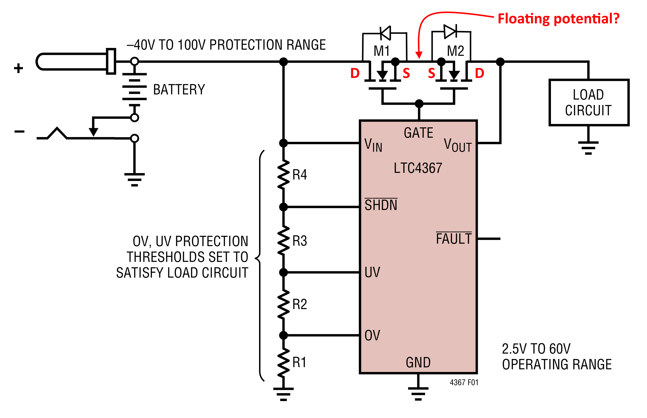
Please consider an exemplary back-to-back MOSFET N driver IC (drew the body diodes of M1 and M2 for clarity):

enter image description here

I understand how is it possible to turn off the M1/M2 transistors from the gate voltage point of view (since its higher than VIN voltage due to the internal charge pump). What I do not grasp is why do the transistors turn on when the gate voltage goes high and VIN voltage appears, since the sources of the transistors are "floating". The sources potential is not fixed to voltage value (lower than the gate voltage) before the M1 starts conducting. Question is, why does it start conducting in the first place? How to understand this phenomena?

\$\endgroup\$
1

4 Answers 4

6
\$\begingroup\$

FETs have a neat party trick: they can conduct in both directions. And, a bias on gate-to-drain will turn on the FET as well as the more customary gate-to-source.

In this circuit then, the left-hand FET will be on, bringing up the source for both: the two sources will be at the same voltage as the left-hand FET drain. So the right hand FET will also be on.

This slide deck gives more information about how FET biasing works. tl, dr: it’s about gate to substrate bias. https://alan.ece.gatech.edu/ECE3040/Lectures/Lecture24-MOS%20Transistors.pdf

One detail: the IC brings the gate voltage above both FET drain and source voltages since n-FETs are being used. This ensures that turn-on will occur, since Vgs is higher than threshold.

\$\endgroup\$
8
  • \$\begingroup\$ Thabks for the answer. I did not know about this phenomena. I was convinced that only by taking the gate higher than the source the transistor turns on (bo matter the 2 direction co ductivity). In here my explanation was that the M1 body diode that has leakage current, which causes the M1 source to be VIN - drop, and thats why it works. Could you give some references on the draid biasing? \$\endgroup\$ Commented Apr 30, 2022 at 5:54
  • 1
    \$\begingroup\$ FETs are at their basis symmetric devices. The body diode only comes about because of tying the source to the body, forming a parasitic p-n junction. \$\endgroup\$ Commented Apr 30, 2022 at 17:09
  • \$\begingroup\$ This slide deck may help: alan.ece.gatech.edu/ECE3040/Lectures/… \$\endgroup\$ Commented Apr 30, 2022 at 17:19
  • \$\begingroup\$ thank you for the reference. However I could not find there the info about the issue at hand- it is always referenced as gate voltage vs source voltage still. \$\endgroup\$ Commented May 1, 2022 at 9:22
  • 1
    \$\begingroup\$ Yes, exactly. There’s such a thing as a 4-terminal FET with a separate body connection. \$\endgroup\$ Commented May 6, 2022 at 0:49
2
\$\begingroup\$

If you read the datasheet, the IC has a charge pump that produces 13.1V above Vout and the common source node never floats more than M2's body diode drop above Vout.

\$\endgroup\$
6
  • \$\begingroup\$ Thanks for the answer. I understand the higher gate voltage concept. I do not grasp why does the M1 turn on if the source is floating. \$\endgroup\$ Commented Apr 29, 2022 at 21:46
  • 1
    \$\begingroup\$ @ŁukaszPrzeniosło M2's body diode keeps the source node voltage to a maximum of Vout + Vd. The charge pump outputs a voltage referenced/relative to Vout. If the MOSFET requires Vgs = Vgs_Rdson to conduct, then as long as the charge pump outputs Vgs_Rdson + Vd then there is always enough voltage to cause M1 to conduct. \$\endgroup\$
    – DKNguyen
    Commented Apr 29, 2022 at 22:00
  • \$\begingroup\$ Still, this is not about the gate voltage. Its about why the M1 can be turned on, if its source is not biased to any voltage in the beginning off state. \$\endgroup\$ Commented Apr 30, 2022 at 5:55
  • \$\begingroup\$ But it is. Did I not just say the source voltage is always between Vout and Vout + Vd? Vout still has a voltage relative to GND even when unpowered, whatever it maybe, even if it is not predictable. I think you're mistaking application of a voltage to absence of a voltage. Just because I am not explicitly applying a voltage between two points does not mean that a voltage does not exist between those two points. The source voltage here may not be deterministic but we know it is always between Vout and Vout+Vd which is all we need to know. \$\endgroup\$
    – DKNguyen
    Commented Apr 30, 2022 at 15:51
  • \$\begingroup\$ When the gate is at 0V, the voltage at the sources is 0V as well. So it seems that it is not in a float state, but instead in a fixed 0V state, but I don't know why (measured this with a multimeter). Also, what do you refer to as Vd? Drain voltage- if yes, which drain? The one on the load side (since the other one is VIN)? \$\endgroup\$ Commented May 1, 2022 at 9:27
2
\$\begingroup\$

A reverse diode still conducts, with \$I = I_s(e^{V/V_f}-1)\$. At significantly reverse bias, the current is the saturation (leakage) current. At no time is the common node floating, it is just high impedance.

\$\endgroup\$
1
\$\begingroup\$

Because the FET has a reverse diode from S to D, the S of the 'other' FET cannot be more than 0.7 V above that drain. So, the common S node is no higher than the lowest of either drain. Therefore if GATE is lower than both drains, then both FETs will be off.

Consider M2. and a load at 10 V. Therefore SS can't be higher than ~ 10.7 V. now if the GATE is at 0V, M2 will be OFF, and S can remain no higher than 10.7 V. If VBATT is higher than 0 V, M1 will also be off and will provide the desired blocking.

Note that node SS can now be at any votlage between ~ 10.7 V and 0 V -- it is floating in that range. but no matter what value it is at, M1 will be off, so no curent can flow. M2 will be off also.

This is not acomplete circuit. FETs need their VGS held to less than 10 V (usually), and you cannot have VG-D more than that either (you can have VD-G mucch higher). Thus you usually have a zener ciruit to limit VGATE to no more than 10 V above the lowest of drain1, drain2, and no more than 10 V below the lowest V either.

\$\endgroup\$
5
  • \$\begingroup\$ Thank you for answer. I still do not get it, and here I mean the very first turn on. Assume a no voltage presence state. The voltage is applied to VIN. GATE goes to a level VIN + 10 V, so the M1 can turn on- the thing I don't understand is: why does it turn on, if its source is not tied to any specific potential, but floating? \$\endgroup\$ Commented Apr 29, 2022 at 21:45
  • \$\begingroup\$ @ŁukaszPrzeniosło With an initial "no voltage presence state" Vout will also be 0V and the Source node will be <0.7V. I wouldn't call that floating. \$\endgroup\$ Commented Apr 29, 2022 at 22:01
  • \$\begingroup\$ But for any voltage to be present on the sources (0, lower or higher), there must be current flow from the M1 drain- is there any? \$\endgroup\$ Commented Apr 30, 2022 at 5:57
  • \$\begingroup\$ @ŁukaszPrzeniosło If a circuit has a dead end resistor sticking out of it, and the end connected to the circuit measures 5V relative to GND, what's the voltage on open end of the resistor even though there is no current flowing through the resistor? electronics.stackexchange.com/questions/98322/… \$\endgroup\$
    – DKNguyen
    Commented May 1, 2022 at 1:51
  • \$\begingroup\$ Im not sure this is the same case. If we thread the transistor D-S patch as a resistor, then in the off state, we should have VIN at the sources. That is not the case. In off state, the potential measured at the sources is 0 V... \$\endgroup\$ Commented May 1, 2022 at 9:24

Your Answer

By clicking “Post Your Answer”, you agree to our terms of service and acknowledge you have read our privacy policy.

Not the answer you're looking for? Browse other questions tagged or ask your own question.