I'm considering designing my own U.2 to M.2 converter card to make use of the four U.2 (PCIe 3.0 x4) connectors on my motherboard. Commercial products are available for doing this type of conversion, such as this one from StarTech, but the PCB design looks amateurish, the pricing for four of them is excessive, and I'm not a fan of them taking up a whole 2.5" SSD form factor just for a single drive. AliExpress has similar devices for much lower prices, but they don't solve the other issues.
From what I can tell, these cards are essentially just splicing the connections and providing a higher current 3V3 rail from the U.2's 12V0 rail. The BoM is small and the layout isn't particularly challenging at PCIe 3.0 speeds, so that's well within my capabilities. 85 ohm controlled impedance for the diffpairs, minimise high speed trace lengths to keep losses low, keep the inter-pair and intra-pair timing skew as short as possible, solid ground reference planes on the inner layers, buck converter kept far away from the PCIe traces, probably a solid 3V3 polygon on the bottom layer for lower PDN impedance, low inductance (0402) decoupling caps right on the M.2 connector.
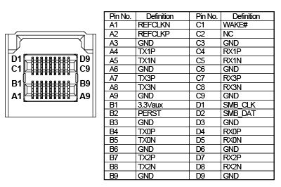
The connector standards are a little confusing, but I believe the "internal U.2" connector is a SFF-8643 Mini-SAS HD connector, such as Amphenol G40H11331HR, but with a different pinout to typical SAS usage. It was rather difficult to navigate the connector info and find a pinout, and I had to resort to digging them out of product manuals to find anything vaguely concrete. This was the best I could find:
Based on this and the M.2 key M pinout, it seems like I simply need to connect the PCIe lanes, REFCLKN/P, PERST, (PE)WAKE#, and the SMB pins from the SFF-8643 to the M.2 socket, tie the incoming 12V0 pins together since they'll all be on the same power domain from the motherboard, then use a LT7200S for generating the high current 3V3 rails. I'm assuming around 10W peak load per M.2 device based on published specs by NVMe SSD vendors, so roughly 3.1A on each 3V3 rail. I'm currently leaning towards operating the LT7200S in multiphase mode to generate a single 3V3 rail instead of four separate rails, to simplify power delivery in the PCB layout. The downside is that it'll always power all of the installed M.2 cards even if only one cable is connected, but since this is a one-off design for my own use I'm not too worried about that.
The downstream M.2 slots have some additional pins that aren't present on the U.2 connections. Based on the info in M.2 For Hackers, my understanding is that I should pull CLKREQ# to GND, leave SUSCLK floating, and I can feel free to ignore DAS/DSS and leave that floating. Since the CONFIG lines are set by the M.2 devices, and the U.2 ports don't do anything with them, my assumption is that I can ignore those too. DEVSLP is only used by SATA devices, but it seems like pulling it low would be a good move.
Existing U.2 to M.2 adapter cards don't seem to include a supervisor IC to ensure that the incoming 12V0 rail is stable before turning the buck reg on, but their DC-DC converters (and, presumably, input caps) aren't anywhere near as beefy as in this design, so I wonder if I might want to include a PMIC to provide PGOOD to the RUNx pins on the LT2700S and perhaps limit inrush current.
Does all of this sound correct and sensible, including the pinout diagram above? Have I missed anything important?

