I'm looking for the correct pcb footprint for the MAX1979 IC by Maxim, supposedly in a TQFN-EP package. While the land patterns are available on Maxim's website, there are apparently several 48 lead TQFN packages with different footprint areas, and the only information on the IC datasheet is that the area is below 0.93 in² (not very helpful). Where can I find the exact dimensions of the package?
2 Answers
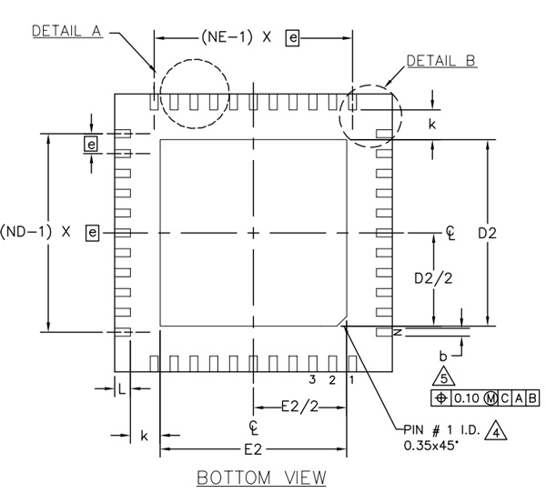
The physical pin layout for the part is provided in this document, linked from page 19 of the datasheet.
The detailed dimensions are given in the package drawing document:
 .
.
The separation of package drawing document from part datasheet is common with many Maxim parts, and also with some other manufacturers.
What Anindo posted is NOT the foot print, but rather an inverted view of the package. DO NOT make your footprint from this.
Unfortunately it looks like instead of just giving you the information in the data sheet like most IC manufacturers, you're going to have to download an Ultra Librarian package reader software, then download the corresponding part from Maxim. The good news is that if you're using a big name software suite you can just download the symbol/land and import it directly, but buyer beware (as usual).
Maxim's site for CAD symbols and land patterns (there is also a link for free UL reader software). http://www.maximintegrated.com/en/design/packaging/cad/
From there a search for MAX1979 will return about a half dozen or so results. Check them against the model number of the IC you order and then you'll have the correct land pattern.
-
\$\begingroup\$ There is nothing wrong with making a footprint from the bottom view of the package. All of the dimensions are there, and there is no screwing around with downloads required. \$\endgroup\$ Commented Jul 7, 2014 at 12:39
-
2\$\begingroup\$ Interesting: While I was wrong in using the term "land pattern" in my answer, I just discovered that the diagram I posted actually does correspond to the footprint (flipped due to bottom view), while a land pattern is the copper pattern: "moving forward into the future we (the IPC) have found it useful to refer to them as "land patterns" and use the name "footprint" in a different way. You can think of a footprint as what you would see if you picked up a component and pushed it into sand or clay, the imprint it leaves would be its footprint, which is its actual physical size." (contd...) \$\endgroup\$ Commented Jul 7, 2014 at 12:42
-
1\$\begingroup\$ ... "The land pattern on the other hand describes the size of the pads needed to solder the leads to the board, which have wildly differing dimensions depending on what you are trying to do (wave soldering, reflow, high-density, etc.). So for a given part it will have one footprint but maybe several land patterns.". \$\endgroup\$ Commented Jul 7, 2014 at 12:42
