4
\$\begingroup\$

I'm currently trying to learn and understand about creating an H-Bridge using two half bridge drivers. The half bridge drivers I have are IR2184.

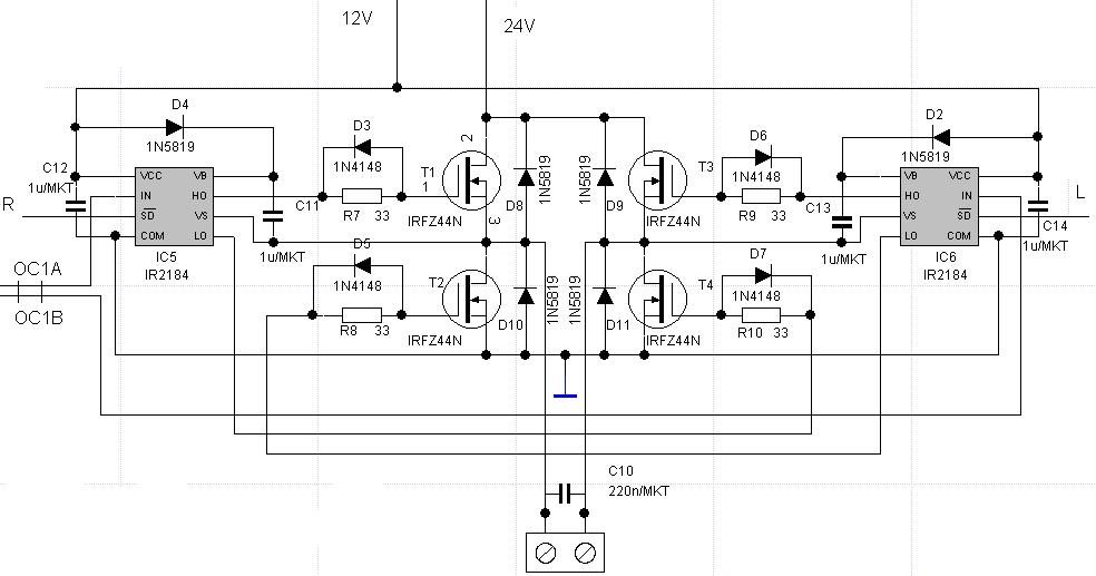
I found a circuit diagram someone else has designed using the same driver ICs but I have some questions about it.
Someone else's circuit diagram

I've seen several similar circuits where resistors are placed in line with the gates of the mosfets - What are those resistors for?

Also on the circuit above the designer has placed some diodes parallel to those resistors. Is there a reason for doing that?

\$\endgroup\$

4 Answers 4

5
\$\begingroup\$

You should always provide a gate resistor.

At the very least it actually helps define the current that will flow in and out of the GATE during switching transients (to charge and discharge the gate capacitance).

Without any gate resistor you could have very large (relatively speaking) peak currents flowing. Best-case... its an EMC concern, worst-case... you potentially burn out the gate of the FET.

You also run the risk of creating a Pierce Oscillator.

In this instance you can see a series gate resistance with a diode in parallel. This limits the current and thus the switching time for TURN-ON.

The diode then "shorts" the resistor out permitting a higher charge transfer for a TURN-OFF.

This is a cheap/simple means to mitigate shoot-through's of a H-bridge leg during PWM transitions as you now have fast TURN-OFF and slow TURN-ON

\$\endgroup\$
5
\$\begingroup\$

There's another important reason to the presence of the diode antiparalled to the gate resistor. In a bridge configuration, when a transitor goes on the switching, the voltage acroos the other transitor has a increased dV/dt.

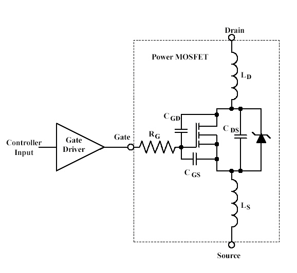
In a MOSFET, that's the case of your H-brigde, there's three intrinsic capacitances composing its body, like in the image below (that shows other stray components of the Mosfet body):

The MOSFET's capacitances

When the Vds voltage increases, all the three capacitances need to be charged, like in the schematic below:

schematic

simulate this circuit – Schematic created using CircuitLab

Where the red arrows are current flowing through the circuit (when Vds are increasing).

So, if this resistance of the discharge isn't low, the Cgs capacitange could had a peak of charge, creating a short-time short-circuit, named punch through.

More information at this app. note

http://www.irf.com/technical-info/appnotes/an-936.pdf

\$\endgroup\$
4
\$\begingroup\$

The resistors in series with the MOSFET gates are damping resistors. They reduce the tendency of the circuit to oscillate or ring when switching.

The diodes in parallel look like they are intended to speed up the discharge of the MOSFET's gate capacitance when the signal goes from HIGH to LOW. So, they help the MOSFETs switch off faster.

\$\endgroup\$
3
\$\begingroup\$

Because FET input has gate capacitance, and the driver usually has strong current source capacity. So, when with no resistor, the current spike may cause EMI problem, and other problems. So adding series resistor to slow-down the switching.

But usually, we needs to shut down the FET faster, adding of the damping resistor will slow down the discharging of the gate capacitance too. With reverse paralleled diode, when the gate capacitor discharge, the current will flow in the diode, but not the damping resistor, this makes the shut down faster than turning on.

\$\endgroup\$

Your Answer

By clicking “Post Your Answer”, you agree to our terms of service and acknowledge you have read our privacy policy.

Not the answer you're looking for? Browse other questions tagged or ask your own question.