3
\$\begingroup\$

I am programming a TWI slave based on an ATMEGA644PV.

It is working in general, the master can send and read data from the slave. So far so good.
But on some read-requests, the slave requires "more time" to prepare the data. I would like to utilize clock stretching to make the master wait until the data is ready.

The ATMEGA datasheet points out:

The Slave can extend the SCL low period by pulling the SCL line low. This is useful if the clock speed set up by the Master is too fast for the Slave, or the Slave needs extra time for processing between the data transmissions.

This is exactly what I want, but I don't get how to implement this on the driver level. I see no way to indicate to the I2C slave hardware that it shouldn't immediately ACK, but instead pull the SCL for a period of my choice.

From what I get, I can only tell the slave to ACK or - well - not to ACK at all after being addressed or a data byte being transferred.

Am I missing something obvious here? This is the first time I look at I2C from the view of a slave.

\$\endgroup\$
0

2 Answers 2

4
\$\begingroup\$

The Atmel Atmega processors (including the Atmega644) automatically perform clock stretching whenever the I2C interface needs an action performed by the software.

This action could be when a slave has received a byte of data and the data needs to be removed from the data register before the next byte can be received or when data is needed to transmit. It happens whenever the TWINT flag is set.

The data sheet does not highlight the fact much but it is mentioned in a few places (such as in section 19.5.5 on page 207 on the 02/12 datasheet).

\$\endgroup\$
1
  • \$\begingroup\$ I only have the 9/2015 datasheet, but I think I found what you mean. "While the TWINT Flag is set, the SCL low period is stretched." I totally missed that one. And since the the flag has always to be cleared manually this makes sense. So after receiving the SLA+R adressing, I think will implement a callback from my driver to fill the output buffer BEFORE clearing the flag. Thanks for the pointer, I knew it was something more or less obvious. \$\endgroup\$
    – Rev
    Commented Nov 8, 2016 at 7:21
1
\$\begingroup\$

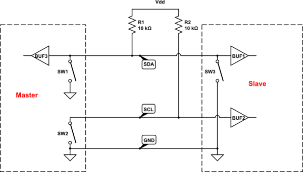
Refer to the following schematic to see the most commonly-used interface between I2C master and slave devices. This interface does not use clock-stretching. The master generates all the clock signals on SCL with SW2 (and the slave only receives these clock signals).
Data can transfer both ways - from master-to-slave with SW1, or from slave-to-master with SW3. Of course, both ends must agree on who can control the SDA data line, to avoid collisions. By "control", I mean that the switch is closed, shorting the data line to ground. An open switch allows the SDA line to rise up to supply voltage through the pull-up resistor. A closed switch has "control" of the SDA line, pulling it to ground (low). An idle bus has all switches open.
schematic

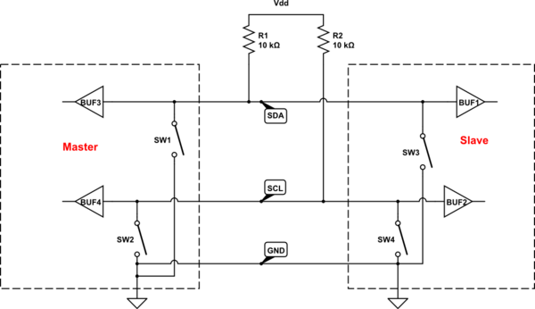
simulate this circuit – Schematic created using CircuitLab In the above schematic, the master clocks SW2 at a rate of 100k cycles-per-second (or 400k for high-speed), expecting the slave to keep up. In a clock-stretched system, the master initiates a clock cycle by closing SW2, and opens SW2 a short time later (that would normally end that clock cycle). But it monitors the clock line with BUF4 to see if R2 has actually pulled back to the idle high state. If the slave switch SW4 keeps the clock line low, that's a clock stretch, holding up further data transfers:
schematic

simulate this circuit A slave device very often has no way to perform a clock-stretch, because SW4 doesn't exist, or if it does exist, there's no way to close it. But any microcontroller has GPIO pins that can do the SW4 function - pulling low to ground. The timing of SW4 is critical: it must be pulled low only while SW2 is also pulling low, to do the slave clock-stretch function. So the pseudo-code for controlling the GPIO pin (SW4) on the slave goes like this:
Initialize GPIO pin to be an input (read). When Slave must clock-stretch, continually monitor GPIO pin, looking for "low". While SCL is low, change GPIO to be output pin, set to logic "0". Keep low until Slave is ready to continue. Once Slave is ready, change GPIO to be input, clearing the clock-stretch.

The ACK or NACK data bit transfer is mostly used to ensure master & slave are alive, and in-sync.

\$\endgroup\$
3
  • \$\begingroup\$ Thanks for the feedback. But I am using the Atmega hardware TWI module. This overrides the GPIO functionality of the pins, thus I have no direct control over them. The question was more about how to use/tell the TWI module that I want to stretch the clock. I am aware of the general principle. \$\endgroup\$
    – Rev
    Commented Nov 8, 2016 at 7:00
  • \$\begingroup\$ @Rev1.0 You can use any GPIO pin as the pull-down clock stretcher - didn't intend you (and wouldn't advise you) to use the I2C clock pin as that GPIO. Use a different GPIO pin. \$\endgroup\$
    – glen_geek
    Commented Nov 8, 2016 at 14:08
  • \$\begingroup\$ Yes, it would probably be possible to use a separate GPIO. However, I already solved the problem according to Kevin's answer. The desired solution was to use the TWI hardware module functions to stretch the clock, which is now working. Thanks anyway. \$\endgroup\$
    – Rev
    Commented Nov 8, 2016 at 14:19

Your Answer

By clicking “Post Your Answer”, you agree to our terms of service and acknowledge you have read our privacy policy.

Not the answer you're looking for? Browse other questions tagged or ask your own question.