I have been looking for weeks for an article or anything that could explain to me how a voltage controlled current source works. I want to know if it's possible to create a VCCS that changes according to a function. What I mean by this is if you can make it so that if the voltage changes according to a function the current changes how you want it to. Can anyone explain to me how a VCCS works and how to make it work according to a function?
-
1\$\begingroup\$ VCCS are mostly used as a theoretical abstractions to model specific circuits, like transistors and amplifiers. Not a real devices. But of course you can come up with something approximating similar behavior physically. \$\endgroup\$– Eugene Sh.Commented Nov 9, 2016 at 16:46
-
\$\begingroup\$ Sort of - most easily in the digital domain, but you can compute some functions with op-amps. \$\endgroup\$– pjc50Commented Nov 9, 2016 at 16:59
-
\$\begingroup\$ Yep, its called a DAC \$\endgroup\$– Voltage Spike ♦Commented Nov 9, 2016 at 17:00
-
1\$\begingroup\$ DAC is not a current source... \$\endgroup\$– Eugene Sh.Commented Nov 9, 2016 at 17:02
-
\$\begingroup\$ @EugeneSh., some DACs are. \$\endgroup\$– The PhotonCommented Nov 9, 2016 at 17:05
5 Answers
One possible way to do it:
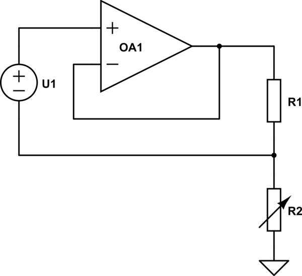
simulate this circuit – Schematic created using CircuitLab
$$I(R_2)=\frac{U_1}{R_1}$$
This works because the current into the + and - inputs of the OP-AMP is zero (by definition) and the voltage between them is also zero (by definition). As the OP-AMP is used as a buffer (- input directly connected to output), the voltage at R1 is U1, so the current through R1 is
$$I(R_1)=\frac{U_1}{R_1}$$
and because there's no way out for that current (by definition), that's also the current through R2. Regardless of the value of R2.
I use this type of voltage controlled current sink for exciting strain gauge bridges and other resistive sensors: -
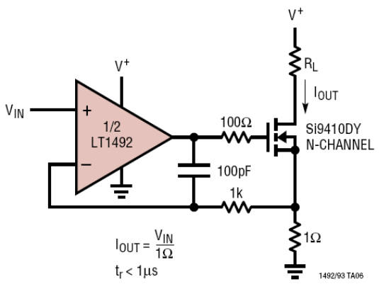
It works by using negative feedback - the current taken by load is sensed by Rsense and the op-amp adjusts the current (if in error) so that the output current is always Vin/Rsense. It has high compliance up to several hundreds of kHz if that is important. To obtain current control down to 0 mA you will need to use an op-amp whose inputs work down to 0V. Also available using a MOSFET: -
The extra two resistors are usually added when the sense resistor is fairly low in value and the gate capacitance becomes somewhat problematic however, most op-amps will drive the MOSFET without the need for the two resistors and extra capacitor.
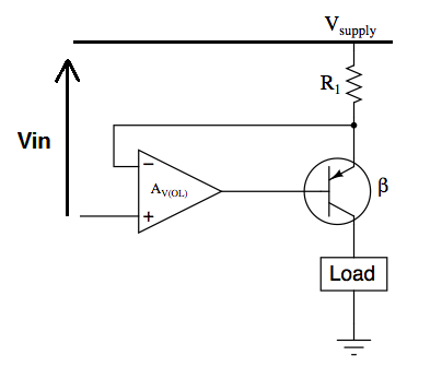
Once you have understood that you can make a current source by using a PNP/Pch transistor connected to the positive rail: -
The down side is that your input reference voltage is relative to the positive rail. You also need an op-amp whose inputs are capable of working at the positive rail so that you can set Iout to be as low as 0 mA.
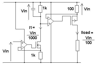
And, you can use another VCCS to obtain a ground reference: -
This uses MOSFETs instead of BJTs and works slightly better in that there is no base current error in the final Iout.
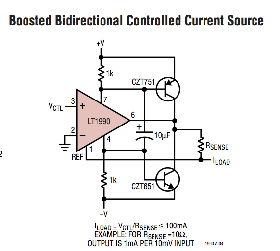
You can even make a bipolar current source using a slightly different topology: -
A voltage controlled current source is a block of components that produces a current (usually) proportional to the input voltage. Real current sources have access to limited voltage so they won't blow up the universe if left open, they'll just limit at the maximum voltage (or maybe arc over some connections).
In order to have a different relationship than proportionality (maybe plus an offset), you can introduce additional elements, usually at the input, but it's also possible at the output, of the current source that have nonlinear behavior. For example, you could have a log amplifier that produced a voltage proportional to the logarithm of the input voltage (with some scaling and offset) and then then feed that voltage to the VCCS to give you a current proportional to the log of the input voltage.
Whether this is done (in between the analog in and out) in the analog domain or digital domain is more-or-less immaterial, at least in theory.
In some cases you might be able to combine the two functions into a single circuit block.
Below is a simple example of a simple and very inexpensive current source that produces an output current that is related to the logarithm of the magnitude of the input voltage (note that it's temperature sensitive so it may not be ideal for precise applications, also the input voltage should be negative only).
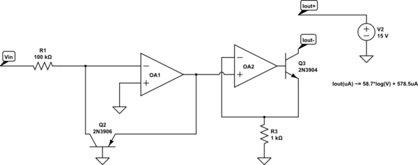
simulate this circuit – Schematic created using CircuitLab
In the above schematic, the output of OA1 is the log-related voltage, and OA2 converts that input voltage into an output current, proportional to the input voltage divided by the emitter resistor R3 value.
There are voltage-controlled current sources (VCCS) in integrated form (of course, non-ideal - with a finite but large output resistance): Operational Transconductance Amplifiers (OTA). If you start a google-search for "OTA" you will see many circuit realizations.
The transfer characteristics (transconductance, g=Iout/Vin) can be controlled with an externally applied current Iabc (amplifier bias current)
Examples: LT1228, Max435, Max 436, LM13600 and LM13700.
More than that, there is a very versatile IC (AD844) which can work as (a) an OTA or (b) as a current-Conveyor (CC) or (c) as a Current-feedback amplifier (CFA).
how a voltage controlled current source works
the voltage changes according to a function [and] the current changes how you want it to
how a VCCS works
how to make it work according to a function
Lots of slightly different questions and I'm not going to take them all on. Since two others have already attempted to use opamps (which are black boxes) and since one direction of your questions might be taken to want to understand how a VCCS works, I thought I'd provide a few more primitive thoughts to show you why opamps are often used to create more generalized forms. You can then decide which direction you want to take in learning more.
Probably the most primitive (one part) form of an imperfect VCCS is just a BJT:
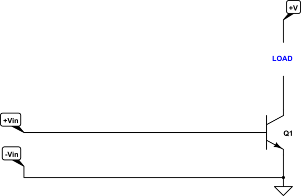
simulate this circuit – Schematic created using CircuitLab
Here, you can apply a voltage between the base and emitter and this will control the current through the LOAD shown there.
There are lots of problems, though:
- The required voltage is proportional to the logarithm of the desired current. Spehro has made use of this fact in his circuit, in fact. So whether or not this is desirable is a matter of what you are trying to do.
- The source voltage must also provide sufficient base current to handle the BJT's recombination current in the base region.
- The required voltage is also temperature-dependent. So the current will vary quite a bit with only small changes in the BJT temperature.
- The required voltage also varies by individual part and part family.
- The Early Effect also affects the output current.
- It only works with positive voltages (NPN here) over a narrow range.
- At low output currents (relative to the nominal range for the BJT), recombination of carriers at the surface and in the emitter-base space-charge layer, plus the formation of emitter-base surface channels, also affect the output.
- At high output currents, the growing significance of injected minority carriers into the base region also affects the output current.
One of the more pronounced problems is that very tiny changes in the base-emitter voltage lead to large changes in the collector current. And there are more effects, all of which make it fairly difficult to use without wrapping it with a closed loop control system (which entirely removes the advantage of being a single part.)
It's rare to see this applied, except in circuits such as Spehro's (not so common) or in current mirrors (very common.)
An improvement can be easily had, though. You can include a resistor in the emitter leg:
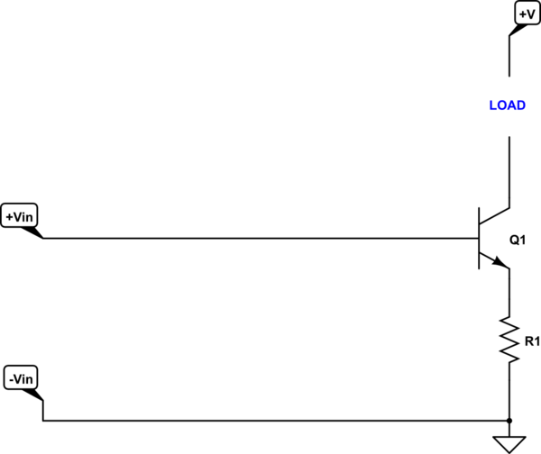
In this case, the input voltage (less a \$V_{BE}\$ drop) is applied across the emitter resistor. This causes a specific emitter current that depends upon that voltage, which is then available (most of it) for the LOAD. No longer is the control voltage proportional to the logarithm of the desired current -- but now there is a simple proportionality between the two that is expressed by \$R_1\$as in: \$I_{OUT}\approx \tfrac{1}{R_1}\cdot\left(V_{IN}-V_{BE}\right)\$. The resistor provides a local, negative feedback here, which is why this works. Using local negative feedback makes this is a lot more useful in an otherwise open-loop situation. Relevant voltages for this circuit are often a lot easier to apply (than in the first case.)
This circuit also has many of the problems of the earlier circuit. But their impact is often reduced quite a bit. For example, it is still temperature-dependent. But since this impacts \$V_{BE}\$ and since \$V_{BE}\$ is often only a small percentage of the supply voltage, the current varies much, much less from a designed value than in the first case.
Circuits become much, much more complex before you start getting closer to an ideal VCCS. No circuit reaches the ideal, of course. But over some desired range of operation, they can do a credible approximation of one.
I've shown you just two very simple cases with BJTs. It's possible to do similar things with MOSFETs and JFETs. The details vary, as do the problems that may complicate a resulting solution circuit. This is one of the reasons why designers reach for opamps here. Much of the heavy lifting work (as well as the myriad advantages that come when you are designing an entire circuit on the same substrate; only one of which is that nearby temperatures can be taken is similar) has been done for you and where you have very large values of open loop gain to apply in a closed circuit to achieve your goals.
The main point here is that, within a limited range of input voltages and output currents and to some reasonable approximation, a VCCS can be had. But like anything else in the real world, it's all a matter of balancing appropriate compromises. Ideals, in the macro-world we live in (as opposed to the quantum world we don't), don't exist. But we can work to get arbitrarily close, when that is important enough.


